Welcome to the power supply design tips! With the emphasis on the need for more efficient, lower-cost power solutions, this article presents some tips to help you with various power management topics. Whether you're in the power business for many years or just stepping into the power supply, you can find some extremely useful information here to help you meet your next design challenge.
Tip One to choose the right working frequency for your power supply
Choosing the best operating frequency for your power supply is a complex trade-off process that includes size, efficiency, and cost. In general, low frequency designs tend to be the most efficient, but they are the largest and most costly. Although increasing the frequency can reduce the size and reduce the cost, it will increase the circuit loss. Next, we use a simple step-down power supply to describe these trade-offs.
We start with a filter component. These components occupy most of the power supply volume, while the size of the filter is inversely proportional to the operating frequency. On the other hand, each switching conversion is accompanied by energy loss; the higher the operating frequency, the higher the switching loss and the lower the efficiency. Second, higher frequency operation usually means that smaller component values ​​can be used. Therefore, higher frequency operation can bring significant cost savings.
Figure 1.1 shows the relationship between the frequency and volume of the buck power supply. At 100 kHz, the inductor occupies most of the power supply (dark blue area). If we assume that the inductor volume is related to its energy, then its volume reduction will be proportional to the frequency. The above assumptions are not optimistic in this case because the core loss of the inductor at a certain frequency is greatly increased and the size is further reduced. If the design uses ceramic capacitors, the output capacitor volume (brown area) will decrease with frequency, ie the required capacitance will decrease. On the other hand, input capacitors are often chosen because of their ripple current rating. This rating does not change significantly with frequency, so its volume (yellow area) can often be kept constant. In addition, the semiconductor portion of the power supply does not change with frequency. Thus, passive devices can occupy most of the power supply volume due to low frequency switching. When we switch to a high operating frequency, the semiconductor (ie, the semiconductor volume, the light blue region) begins to occupy a large proportion of space.
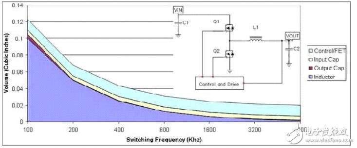
Figure 1.1 The size of the power supply components is mainly occupied by semiconductors.
The graph shows that the semiconductor volume does not vary with frequency in nature, and this relationship may be oversimplified. There are two main types of semiconductor-related losses: conduction losses and switching losses. The conduction losses in synchronous buck converters are inversely proportional to the die area of ​​the MOSFET. The larger the MOSFET area, the lower its resistance and conduction losses.
The switching loss is related to the speed of the MOSFET switch and how much input and output capacitance the MOSFET has. These are all related to the size of the device. Large volume devices have slower switching speeds and more capacitance. Figure 1.2 shows the relationship between two different operating frequencies (F). The conduction loss (Pcon) is independent of the operating frequency, while the switching losses (Psw F1 and Psw F2) are proportional to the operating frequency. Therefore, a higher operating frequency (PswF2) results in higher switching losses. When the switching loss and conduction loss are equal, the total loss per operating frequency is the lowest. In addition, as the operating frequency increases, the total loss will be higher.
However, at higher operating frequencies, the optimum die area is smaller, resulting in cost savings. In fact, at low frequencies, minimizing losses by adjusting the die area results in a very costly design. However, after moving to a higher operating frequency, we can optimize the die area to reduce losses, thereby reducing the semiconductor footprint of the power supply. The downside to this is that if we don't improve semiconductor technology, power efficiency will decrease.
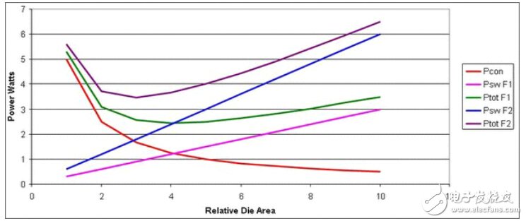
Figure 1.2 Increasing the operating frequency results in higher overall losses
As mentioned earlier, a higher operating frequency reduces the inductor volume; the required inner core plate is reduced. Higher frequencies also reduce the need for output capacitance. With ceramic capacitors, we can use lower capacitance values ​​or less. This helps to reduce the area of ​​the semiconductor die, which in turn reduces costs.
The secret is to control the noise power supply
Noise-free power supplies are not accidentally designed. A good power layout is designed to minimize experiment time. Taking minutes or even hours to look at the power layout carefully can save you days of troubleshooting time.
Figure 2.1 shows the block diagram of some of the main noise-sensitive circuits inside the power supply. The output voltage is compared to a reference voltage to generate an error signal, which is then compared to a ramp to generate a PWM (Pulse Width Modulation) signal for driving the power stage.
Power supply noise comes mainly from three places: error amplifier input and output, reference voltage, and ramp. Careful electrical and physical design of these nodes helps minimize troubleshooting time. In general, noise is capacitively coupled to these low level circuits. An excellent design ensures tight layout of these low level circuits and away from all switching waveforms. The ground plane also has a shielding effect.
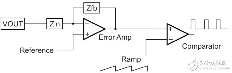
Figure 2.1. Many noise formation opportunities for low-level control circuits
The error amplifier input may be the most sensitive node in the power supply because it typically has the most connected components. If you combine it with the extremely high gain and high impedance of this stage, you will have endless troubles. During the layout process, you must minimize the length of the node and place the feedback and input components close to the error amplifier as close as possible. If there is a high frequency integrating capacitor in the feedback network, you must place it close to the amplifier and the other feedback components follow. Also, a series resistor-capacitor may also form a compensation network. The most ideal result is to place the resistor close to the input of the error amplifier, so that if a high frequency signal is injected into the resistor-capacitor node, then the high frequency signal has to withstand a higher resistance impedance - and the capacitor has a high frequency signal The impedance is small.
Slopes are another potential source of noise problems. The ramp is typically generated by capacitor charging (voltage mode) or by sampling (current mode) from the power switch current. In general, the voltage mode ramp is not a problem because the impedance of the capacitor to the high frequency injected signal is small. Current ramps are tricky because of rising edge peaks, relatively small ramp amplitudes, and power stage parasitics.
Figure 2.2 shows some of the problems with current ramps. The first image shows the rising edge peak and the resulting current ramp. The comparators (according to their different speeds) have two voltage nodes (potenTIal trippoints), and the result is an out-of-order control operation that sounds more like a fried bacon. This problem can be well solved by using rising edge blanking in the control IC, which ignores the initial portion of the current waveform. The high frequency filtering of the waveform also helps to solve this problem. Also place the capacitor as close as possible to the control IC. As these two waveforms show, another common problem is subharmonic oscillation.
This wide-narrow drive waveform appears to be insufficient slope compensation. Adding more voltage ramps to the current ramp will solve the problem.
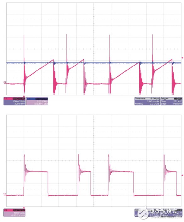
Figure 2.2 Two common current mode noise problems
Although you have designed the power layout quite carefully, there is still noise in your prototype power supply. What should I do? First, you have to make sure there is no problem with the loop response that eliminates the instability. Interestingly, the noise problem may look like instability at the crossover frequency of the power supply. But the real situation is that the loop is correcting the injection error with its fastest response speed. Again, the best approach is to identify that noise is being injected into one of three places: the error amplifier, the reference voltage, or the ramp. You only need to solve it step by step!
The first step is to check the nodes to see if there is significant nonlinearity in the ramp or if there is a high frequency change in the error amplifier output. If no problems are found after the inspection, the error amplifier is removed from the circuit and replaced with a clean voltage source. This way you should be able to change the output of this voltage source to smoothly change the power output. If this works, then you have narrowed the problem down to the reference voltage and error amplifier.
Sometimes, the reference voltage in the control IC is susceptible to the switching waveform. This situation may be improved by adding more (or appropriate) bypasses. In addition, using a gate drive resistor to slow down the switching waveform may also help to solve this problem. If the problem is with the error amplifier, then the compensation component impedance will be reduced.
This helps because it reduces the amplitude of the injected signal. If all of these methods do not work, then the error amplifier node is removed from the printed circuit board. Air wiring the compensation components helps us identify where there is a problem.
According to the working frequency response ranges, speakers can be classified into tweeters, mid ranges, woofers and full ranges.


FAQ
Q1. What is the MOQ?
XDEC: 2000pcs for one model.
Q2. What is the delivery lead time?
XDEC: 15 days for normal orders, 10 days for urgent orders.
Q3. What are the payment methods?
XDEC: T/T, PayPal, Western Union, Money Gram.
Q4. Can you offer samples for testing?
XDEC: Yes, we offer free samples.
Q5. How soon can you send samples?
XDEC: We can send samples in 3-5 days.
Speakers By Frequency,High Bass Speakers,Small Loudspeakers,High Frequency Speaker
Shenzhen Xuanda Electronics Co., Ltd. , https://www.xdecspeaker.com