In general, designers will find continuous approximation register (SAR) and ΔΣ analog-to-digital converters (ADCs) in lower frequency applications. The signal chain for these applications typically begins with a sensor that produces a low output voltage or current signal. These signals must be amplified and filtered before they can be digitized. It can be seen that the SAR and ΔΣ converter signal paths adjust the low sensor signals in very different ways. This article will explain the various signal characteristics that represent the sensor and the signal chain components of each converter type. For signal characteristics, this article explores the application requirements for each converter type and what is appropriate for these converters.

Sensor electrical characteristics analysis
The signal chain for the sensor application starts with the sensor. Figure 1 shows several sensors that respond to the environment and convert the measured data into electronic signals.
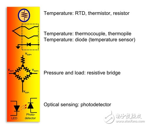
Figure 1 Sensor for SAR and ΔΣ ADC signal conditioning circuits
The analog symbol for the resistance temperature device (RTD) and the thermistor is the resistor. The RTD impedance is relatively small (typically 100 Ohms at 0 °C) and linearly changes at 0.00385 Ohms/Ohm/°C (platinum RTD) and is capable of sensing temperatures between -200 °C and 800 °C. The RTD impedance varies slightly in degrees Celsius. What is the appropriate source of excitation current for RTD components? 1 milliamperes (mA). After the impedance is converted to voltage, the RTD signal will need to be further amplified.
For temperatures between -100 ° C and 175 ° C, a negative temperature coefficient (NTC) thermistor (thermal resistance) produces a higher nonlinear impedance. The typical thermistor impedance at 25 ° C is 10 kOhm. A simple voltage divider that establishes a power supply produces a measurable thermal regulator voltage.
The structure of the thermocouple uses two different metals, such as chrome and copper-nickel alloys (class E) or nickel-chromium and nickel-silicon (class N), two different metals with solder beads attached to one end of the wire. The solder beads are exposed to the heat dissipation environment to cause a temperature difference between the solder beads and the other end of the thermocouple wire. In this environment, an electromotive force (EMF) voltage will appear between the two wires. The EMF voltage can cover tens of millivolts in the temperature range. However, the ΔEMF voltage also reaches tens of millivolts at a one degree Celsius change. The thermocouple also requires the signal gain of the signal path to be digitized.
Engineers use a resistor bridge circuit to simulate pressure and load sensors. When a positive pressure or load is applied to the four-element bridge, the two opposing components will compress and respond, and the other two will become stretched. The designer can apply a voltage or current excitation source to the high level of the resistor bridge. Although the degree of excitation affects the dynamic range of the sensor output, the maximum difference between VOUT+ and VOUT– is typically between tens and hundreds of millivolts.
Photodiodes and associated preamplifiers are the link between basic optical activity and electronics. Light sensing circuits are used in systems such as computed tomography (CT) scanners, blood analyzers, smoke sensors, position sensors, infrared pyrometers, and chromatographs. In these circuits, the photodiode produces a small current from the nanoamperes to the microamperes, which varies in proportion to the illuminance. The preamplifier converts the current output signal of the photodiode sensor to a usable voltage level.
All of the sensors described above require excitation source and signal conditioning circuitry to convert small signals to the level of voltage available to analog converters at the end of the signal path. The general signal chain of a SAR analog-to-digital converter and a ΔΣ analog-to-digital converter will be described below.
SAR-ADC signal path
SAR converter signal chain from sensor to microcontroller (MCU) or microprocessor (MPU), including signal conditioning stage, analog gain stage, anti-aliasing filter (AAF), SAR driver amplifier and SAR converter (figure 2).
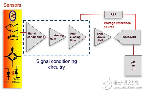
Figure 2 SAR-ADC Signal Path--The bias sensor signal is amplified and filtered to provide the appropriate input signal for the SAR converter.
The signal conditioning stage provides the necessary sensor bias stage voltage shift. In this signal path, the analog gain stage is used to make the voltage output range of the sensor conform to the input range of the SAR converter. In this way, the designer can make full use of the number of bits in the converter. For example, if the sensor produces a total output range of 50 millivolts and the input range of the analog digital converter is 5 volts, the analog gain required for such a specific gain stage is ~100V/V. The analog device type for this circuit location is an op amp or instrumentation amplifier.
In Figure 2, the analog gain stage is followed by an anti-aliasing filter. This å- to fifth-order anti-aliasing (analog) filter removes the superimposed analog signal noise before the signal is sent to the SAR converter. Before the signal becomes a digital block, the AAF will reduce the high frequency noise that will alias back to the digital signal. Analog filtering is an important part of the data acquisition system. If the analog filter is not used, the signal outside the analog-to-digital converter sampling bandwidth will be aliased back to the signal path. Once the signal is aliased during the digitizing process, it is not possible to distinguish noise in the frequency band and out of band.
The SAR driver amplifier sends the signal to the SAR analog-to-digital converter. This driver amplifier has tremendous drive capability to deliver a stable signal to the converter. Once the SAR analog-to-digital converter produces the final digit block, the microcontroller or microprocessor will further perform signal filtering to convert the signal to a usable digital value. SAR converters are a common architecture for media parsing applications. The resolution of the SAR analog-to-digital converter is between 8-bit and 18-bit, and the sampling speed is less than 10MSPS.
Surround Speakers,Wall Hanging Speakers,Home Theater Speakers,Ultra Thin Wall Hanging
The ASI Audio technology Co. Ltd , https://www.asi-sound.com