This application note provides general information about the network interface and circuit designs for secondary protection of the DS2155 SCTs. These designs are targeted for compliance with the following standards, Underwriters Laboratories UL 1950 and UL 60950, TIA / EIA-IS-968, Telcordia GR 1089-Core and International Telecommunication Union ITU-T K.20, and K.21.
Gas discharge tubes or carbon blocks located at the point where the line enters the premises usually provide primary voltage protection; but because primary voltage protection only limits the voltage surges to 1000V peak and power-line cross to 600VRMS, secondary voltage protection is necessary. Secondary voltage protection provides additional voltage and current limiting to prevent damage to the network interface device.
This application note provides general information about the network interface and circuit designs for secondary protection of the DS2155 single-chip transceiver. These designs are targeted for compliance with the following standards:
The circuit in Figure 1 is a traditional interface for T1 / E1 devices and illustrates how resistance is distributed around the transformers. This model will be used as the baseline circuit for the network interface design. It contains extra resistors that are not used in the final design but are essential for many of the concepts presented in this article.
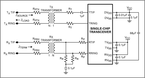
Figure 1. A traditional network interface circuit with distributed resistance for protection.
Receive InterfaceThe receiver inputs present a high impedance and require very little input current to operate. They are designed to recover a signal using a 1: 1 transformer with 0Ω of series resistance under a matched load. The primary consideration in the receive circuit is the accurate termination of the transmission line. A T1 signal is carried on 100Ω balanced twisted pair while an E1 signal is carried on either 75Ω unbalanced coaxial cable or 120Ω balanced twisted pair.
The components involved in the termination network are the RPRX resistors, RR resistors, and the turn ratio of the transformer; the receive-transformer turn ratio is specified as 1: 1, N = 1. The termination circuit is ideal if RPRX is 0Ω and the resistance of RR equals half of the characteristic line impedance. If the RPRX resistors are present, they form a voltage divider and RR must be adjusted. As the resistance of RPRX increases, the resistance of RR decreases. The following equation gives an example of how to calculate RR for proper termination:
ZTERM = RPRX + 2RR / N²
Substitute:
ZTERM = 100Ω, RPRX = 0Ω, N = 1 ∴ 100Ω = 2RR
Solve:
RR ∴ RR = 50Ω
To ease the design of receive termination for both T1 and E1 circuits, the D2155 selects the termination by using software. By designing the receive circuit for 120Ω termination, the internal line interface unit (LIU) can selectively add resistance to the line to achieve the additional termination settings of 75Ω or 100Ω. The LIU inserts either 200Ω or 600Ω of internal resistance between the RTIP and RRING pins.
Changes must be made to the traditional network interface when using internal termination. First, any current-limiting resistors, which include RP and RPRX, must be removed from the receive path. RP must be removed because the resistors interfere with the additional resistance that the internal circuitry adds. RPRX must be removed so the parallel resistance value of 75Ω, 100Ω, or 120Ω is formed by the combination of RR resistors and the internal resistors in the DS2155. Second, the RR resistors must be set to match a line termination of 120Ω. Since RPRX is 0Ω, the resistance of RR equals 60Ω, which is half of the characteristic line impedance.
Finally, because resistance in the circuit can no longer protect the device from overcurrent conditions, a combination of fuses and voltage suppression must be used. An example of this type of circuit along with test results is discussed later.
Note: The 0.1µF capacitor connected to resistors RR form a high-frequency cutoff filter for improved noise immunity and does not affect line termination.
Transmitter Interface The transmitter output drivers present a low impedance and are able to drive sufficient current into the primary winding of the transformer to produce the required output pulse. The transmitter outputs are designed to fit an output pulse into a template based on the line impedance, operational voltage, transformer coil winding, inline resistance, and specific mode of operation, ie, 100Ω T1, 75Ω E1, or 120Ω E1. Unlike the receive transformer, the transmit-transformer turn ratio is directly related to the operational voltage. The DS2155 operates at 3.3V; therefore, the transformer turn ratio is specified as 1: N, where N = 2.
Since the signal pulses and the requirements for the transmit-side interface of T1 and E1 are different, the transmit circuit description is more complicated than the receive circuit. To help users easily understand, the transmitter interface description is broken into two sections. The first section covers the T1 transmitter interface; the second section covers the E1 transmitter interface.
T1 Device Transmit CircuitThe transmitter outputs of Maxim's T1 parts are designed to generate the correct pulse amplitude at the network interface for varying line lengths. Since the different line lengths affect the pulse shape, the parts have programmable output levels. Every part has a transmitter line build-out (LBO) table in the data sheet that shows the settings to choose based on the transformer turn ratio and the line length. A default T1 pulse for a known line length is generated under the following conditions: 3.3V supply; RPTX = 0Ω, RT = 0Ω; and a transmit transformer with a turn ratio of 1: 2.
A nominal 0dB T1 pulse is 3V under a 100Ω load or 3V at 30mA on the network interface. An unprotected circuit using a 1: 2 transformer with 0Ω series resistance will have to produce a 3V × (1/2) = 1.5V pulse at the device's output pins. The current drive into the device side, or primary winding, of the transformer will be 30mA × 2 = 60mA.
Traditionally, resistors RPTX or RT are used to protect the device from surges. But adding series resistance creates a voltage drop that attenuates the output signal pulse. To compensate for the signal loss, select a transformer with a turn ratio larger than 1: 2. This increases the current draw from the transmitter outputs by more than 20%. For this reason, it is recommended that 3.3V circuits be designed with 0Ω of series resistance and other components be used for overvoltage protection.
The following example illustrates how the 1: 2 transformer could be replaced by a 1: 2.42 transformer if it were necessary to use RPTX or RT to protect the circuit from surges. While the current pulse in the network side or secondary winding of the 1: 2.42 transformer will remain the same, the current pulse in the primary winding of the transformer will be 30mA × 2.42 = 72.6mA. Because the output voltage pulse is still 1.5V, the net impedance (RL) seen by the transmitter will be 1.5V / 72.6mA = 20.6Ω and is described by the following:
RL = ZLOAD / N² + 2RPTX / N² + 2RT
Substitute:
RL = 20.6Ω, ZLOAD = 100Ω, N = 2.42
∴ 20.6Ω = 100Ω / 5.86 + 2RPTX / 5.86 + 2RT
Simplify:
3.5Ω = 2RPTX / 5.86 + 2RT
If RPTX is 0Ω, then RT = 1.75Ω, which is not enough to significantly reduce current. However, if RT is 0Ω, RPTX can be as much as 10Ω each and will provide current-limit protection for the transformer.
E1 Device Transmit CircuitThe transmitter outputs of Maxim's E1 parts are designed to generate the correct pulse at the network interface under varying termination conditions. The programmable output levels ensure that pulse amplitude at the network interface have a peak voltage of 3.0V for 120Ω termination or 2.37 V for 75Ω termination. Unlike in T1, E1 applications can have additional resistance in the transmit path to match the source impedance to the characteristic line impedance. The measure of how well the source and line impedance are matched is return loss. A higher return loss results in greater attenuation of line noise or signal reflections being coupled in the transmitter outputs and is calculated by the following:
Return Loss (dB) = 20log10 | ZSOURCE + ZLOAD | / | ZSOURCE-ZLOAD |
ZLOAD = 120Ω or 75Ω and ZSOURCE = 2RPTX + (2RT + 5) × N²
The constant 5 in the ZSOURCE equation above is the transmitter's internal impedance. The return loss for an unprotected network interface without a high return-loss condition is shown below. In the example resistors, the supply voltage is 3.3V, RPTX and RT = 0Ω , the TX transformer has a turn ratio of 1: 2, and the line impedance is 75Ω.
Return Loss (dB) = 20log10 | ZSOURCE + ZLOAD | / | ZSOURCE-ZLOAD |
Substitute:
ZLOAD = 75Ω, N = 2, RPTX and RT = 0Ω
∴ Return Loss = 20log10 | 5 × 22 + 75 | / | 5 × 22-75 |
Return Loss = 20log10 1.73 = 4.7dB
In this example, 58% of the noise or reflected signal can be coupled into the transmitter outputs. To improve the return loss, the value of RT can be increased. Changing RT to a value of 6.2Ω increases the return loss to 28.5dB. This means less than 4% of the inbound signal will be reflected. Because any series resistance will affect the pulse amplitude, the DS2155 compensates for specific RT or RPTX values. When designing the network interface, use Table 1, which is also found in the DS2155 data sheet, for proper transformer and resistor selection. Each setting is based on the operational voltage, the transformer turn ratio, and RT.
Table 1. LBO select for DS2155 3.3V devices
L2 | L1 | L0 | Application | TX Transformer | Return Loss¹ | RT² |
0 | 0 | 0 | 75Ω normal | 1: 2 Step-up | - | 0 |
0 | 0 | 1 | 120Ω normal | 1: 2 Step-up | - | 0 |
1 | 0 | 0 | 75Ω with high return loss | 1: 2 Step-up | > 21dB | 6.2 |
1 | 0 | 1 | 120Ω with high return loss | 1: 2 Step-up | > 21dB | 11.6 |
1. Empty cells indicate that the return loss is less than 21dB.
2. The value of RT shown assumes that RPTX = 0Ω.
To ease the design of transmit-impedance matching for E1 circuits and to allow T1 circuits to take advantage of this feature, the DS2155 performs internal-impedance matching. By designing the transmit interface circuit with 0Ω of series resistance, the internal LIU can selectively add resistance to match the transmitter output to a 75Ω, 100Ω, or 120Ω line impedance. It does this by inserting internal resistance between the TTIP and TRING transmit output driver and the associated pins on the device.
Changes must be made to the traditional network interface when using internal termination. Both the RT and RPTX resistors must be 0Ω. If these resistors are present, the combination of external and internal resistance will cause an impedance mismatch. This end result would be a degraded transmit signal pulse, which will not meet the pulse mask requirements.
A combination of fuses and voltage suppression must be used to protect the device from hazardous transient conditions upon current resistor removal. An example of this type of circuit along with test results is discussed in the following section.
Voltage-Suppression Protection CircuitsThe following secondary voltage protection examples provide immunity from metallic and longitudinal surges as well as power-line cross. The designs in Figures 2 and 3 have several advantages over traditional protection circuits. They decrease the amount of surface area used by components since all of the components used in the design are surface mounted for automated assembly. The components allow low-voltage operation while maintaining the same level of protection as traditional circuits. These circuits allow the use of the new receive-side, software-selected termination and transmit-side line-impedance matching features in the DS2155. Figure 2 is an example of a metallic surge-suppression circuit generally found in customer-premises equipment. Since customer-premises equipment does not have to supply simplex power onto the line, this circuit has the advantage of lower component count and reduced cost. Figure 3 is an example of a longitudinal sur ge suppression circuit usually found in central office equipment. It is common for central office equipment to supply simplex or phantom power to linerepeaters. This is done by applying voltage to the network-side center tap of the transmit and the receive transformer. Because this power connection is longitudinal in nature, it is necessary to ensure that the protection circuit does not activate when this voltage is present.
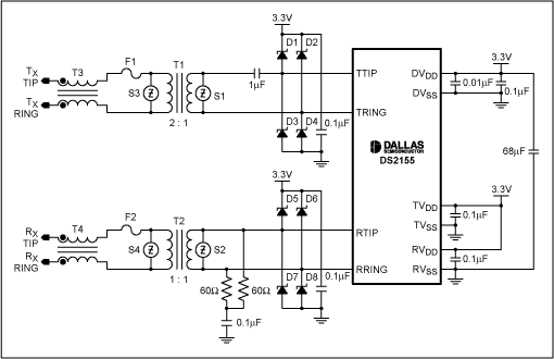
Figure 2. DS2155 network interface circuit with metallic protection and software-selected termination.

Figure 3. DS2155 network interface circuit with longitudinal protection and software-selected termination.
The three main components used for protection are the fuse, thyristor, and Schottky diode devices. The fuse protects the transformer against high current conditions such as power-line cross. The current rating of the fuse is set to match the maximum power dissipation of the transformer. Typical fuses have a surge current rating above 50A for the different voltage and current surge models. If the surge current rating is less than 100A, a current-limiting series resistor will be necessary. One fuse that passes many of the different surge models and does not require current-limiting resistors is the Teccor F1250T TeleLink fuse. The thyristor is a solid-state crowbar device that changes from an open-circuit to a short-circuit condition when the voltage across the device exceeds the switching voltage. The thyristor will remain in the short-circuit state until the current flowing through the device falls below a set-holding current. In the short-circuit state, excess current is routed betwee n the two transmission lines or a transmission line and ground, thus stopping it from damaging the semiconductor device. The Schottky diode is a rectifying device that exhibits large current flows under forward bias and very small current flow under reverse bias. Since the Schottky diodes have a lower forward bias than the internal diodes inside the device, any excess current that would normally flow through the device will now flow through the Schottky diodes.
Table 2. Voltage-suppression protection-circuit components
Reference | Description | Part | Source | Notes |
D1-D8 | Schottky diode | 10BQ040 | International Rectifier | |
F1-F4 | 1.25A slow blow fuse | F1250T | Teccor Electronics | |
S1, S2 | 25V max transient suppressor | P0080SA | Teccor Electronics | |
S3, S4 | 77V max transient suppressor | P0640SC | Teccor Electronics | Figure 2 |
S3ÃS6 | 40V max transient suppressor | P0300SC | Teccor Electronics | Figure 3 |
S7, S8 | 220V max transient suppressor | P1800SD | Teccor Electronics | Figure 3 |
T1, T2 | Transformer 1: 1CT & 1: 2CT (SMT) | PE-68678 | Pulse Engineering | |
T3, T4 | Dual common-mode choke (SMT) | PE-65857 | Pulse Engineering |
1. The layout from the transformers to the network interface is critical. Traces should be at least 20mils wide and separated from other circuit lines by at least 150mils. The area under this portion of the circuit should not contain power planes.
2. Some T1 (never in E1) applications source or sink power from the network-side center taps of the RX / TX transformers. Surge ResultsTo meet the aforementioned specifications, various current and voltage surge pulses must be applied between the tip, ring, and ground conductors. The specific circuit application will determine which surges must be applied to the circuit to pass specification. All of the surges consist of three characteristics: voltage, current, and time. The most common way of referring to a specific surge is by the time, which is expressed in the rise and decay of the surge. The surge is a double exponential, meaning that it rises and decays exponentially. The rise time is measured as the time it takes for the surge to reach the peak current rating, While the decay time is measured as the time when the surge has reached 50% of the peak current rating. Some of the more common surges are 2 × 10µs, 10 × 160µs, 10 × 560µs, and 10 × 1000µs. While there are other su rge combinations, many of those fit inside the template of these four surges. In this case, if the circuit passed the surge that had a larger template, it would theoretically pass any surge that fits inside of that template.
When testing the circuit design, it was decided that the 10 × 1000µs surge would be a sufficient indication of whether or not the circuit would reliably pass and be compliant with the various standards. This was done because of time considerations and the limited availability of the surge generator. Separate 10 × 1000µs surges applied simultaneously to the tip and ring conductors have a peak current of 100A and a peak voltage of 1000V.
Figures 4 and 5 were taken of the surge pulse before they were applied to the network interface circuit. To accurately show the rise and decay of the pulse, a 100x current probe measured the output of the surge generator to ground. Figure 4 shows the rise time of the surge pulse, which is slightly longer than 10µs with no load; the pulse rise time is exactly 10µs when the generator output is loaded. Figure 5 shows the decay time, which is approximately 1000µs.
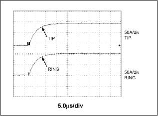
Figure 4. Surge rise time at tip and ring input.
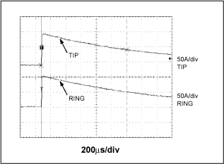
Figure 5. Surge decay time at tip and ring input.
Figures 6 and 7 were taken of the surge pulse as it was applied to the network interface circuit. In both images, trace 1 is the surge measured with 100x current probe from the output of the surge generator to the tip connector. Because the surges on tip and ring are identical and the surge protection is symmetric, it is only necessary to show the surge at one of the connectors. Trace 2 is the surge measured with a 1x voltage probe from the output of the surge generator to the tip connector.
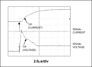
Figure 6. Initial surge clamping at tip input.
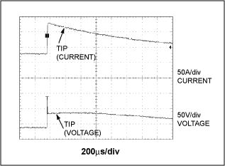
Figure 7. Initial surge voltage spike at tip input.
Figure 6 shows the surge pulse being clamped to a maximum of 178V and a mean of 45V. There is also a slight negative-going pulse that is a byproduct of the surge generator. The residual 45V in the measurement is caused by the inductance of the choke and the large current that is flowing through it. Although it is not shown, the resulting surge on the transformer had a maximum of 178V and was just over 6µs long. The energy contained in this surge is extremely small compared to the original surge present at the tip and ring pins. Figure 7 is the same surge but shows the speed at which the voltage is clamped and the decay of the surge.
One of the main goals when designing telecommunications equipment is to have the equipment remain in working condition after a lightning strike or power cross. The circuits presented in this article will allow telecommunication designs to pass even the most stringent compliance standards. The end result will be equipment that is more stable and requires fewer field repairs, which increases customer satisfaction.
With many years of dedicated R&D in the lighting technology field, Win 3 produces mining Cap Lamps that reduce visual fatigue while maintaining high light output levels.
Win 3 cap lamps outlast the completion. The high quality LED has a lifespan of more than 30,000 hours and the phosphate technology battery more than 1000 cycles.
The lenght of the cable can be customized per customer's request, we usually do 1.6m and 1.8m.
Safety Cap Lamp,Led Safety Cap Lamp,Coal Mining Lights For Sale,Wisdom Led Safety Cap Lamp
ZHEJIANG HUACAI OPTIC-TECHNOLOGY CO LTD , https://www.win3safety.com