This paper mainly introduces the design schematic diagram of three power converters of 3.3V→5V level shifter, analog gain circuit and analog compensation circuit, and briefly explains the circuit diagram.
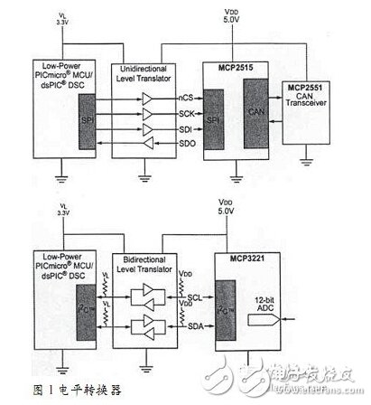
The 3.3V→5V level shifter can directly form level shifting, often with an integrated solution. There are different performance level shifters, with bidirectional and single phase configurations, different voltage conversions and different speeds. Users can choose the best solution according to their needs. Board-level communication between devices (such as MCU to peripherals) often relies on SPI or I2C. For SPI, a unidirectional level shifter is suitable, while for I2C, a bidirectional scheme must be used. Figure 1 illustrates these two options.
3.3V → 5V Analog Gain Circuit The analog gain circuit shown in Figure 2 is used to regulate the analog voltage from a 3.3V supply to a 5V supply. The op amp gain is set for 33KΩ and 17KΩ in the figure. The 11KΩ resistor limits the current that is returned to the 3.3V circuit.
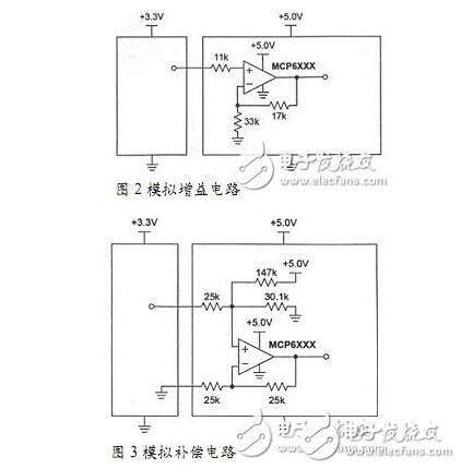
3.3V → 5V analog compensation circuit The circuit shown in Figure 3 compensates for an analog voltage between 3.3V and 5V. This circuit is offset from the 3.3V supply to the 5V supply with an analog voltage. The 147KΩ and 30.1KΩ and +5V supplies are equivalent to a 0.85V voltage source and a 25KΩ resistor and op amp to form a 1V/V gain differential amplifier. The 0.85V equivalent voltage source shifts any signal at the input by the same magnitude. The center signal at 3.3V/2 = 1.65V will also center at 5.0V/2 = 2.50V. The resistor on the upper left limits the current from the 5V circuit.
Cable Box,Junction Boxes,Cable Connection Box,Waterproof Cable Box
Jiangmen Krealux Electrical Appliances Co.,Ltd. , https://www.krealux-online.com