As the number of cars on the road increases, we need more technology to further reduce traffic accidents. In the past few years, the emergence of new system functions based on radar and cameras has made driving safer. Many advanced assisted driving system (ADAS) applications, such as automatic cruise control, road departure warning, traffic signal sign recognition, etc., have become very convenient functions on the vehicle, but have little or no effect on vehicle behavior. However, these technologies are now beginning to play a proactive role in vehicle control, such as lane assisted maintenance (LKA) or automatic emergency braking (AEB), to help achieve the stated goals of reducing traffic accidents. The challenge is that when a system fails, it must be ensured that the system does not cause more damage to the vehicle and the environment.
This article refers to the address: http://
This article takes a single front-end camera system as an example to analyze it in depth and how it can determine critical data streams by using Altera Cyclone V SoC. How to find faults under the existing diagnostic mechanism; and provide some diagnostic examples through flexible Programmable FPGAs enable diagnostics at the system level. In some cases, using custom diagnostics for real-world applications can improve application performance compared to using general-purpose microprocessors, digital signal processing (DSP), and other platforms.
FPGA in ADAS applications
Many of the applications mentioned above have relatively high computational requirements, and feature signals need to be extracted from radar or video images to determine the target and its trace. This usually requires a high performance multicore CPU architecture. These CPUs have the flexibility to reprogram special events, but the disadvantage is that they are less efficient because some features are not required or rarely used.
Power consumption is another factor that needs to be focused on. Many systems are located under the windshield in front of the rearview mirror, exposed directly to the sun, or in the front bumper of the heatsink, so they do not dissipate heat efficiently. When using a multi-core general-purpose CPU architecture running at high frequencies, it is difficult to meet performance and power requirements. These problems can be solved simultaneously using an FPGA. FPGAs typically consume more power than standard logic, but efficient customization of an algorithm actually reduces power consumption compared to general-purpose computing architectures. Another advantage of FPGAs is that when data processing algorithms are implemented, data transfer between internal and external memory can be avoided. If you use an external DDR memory for data processing, the actual power consumption will be very large.
In terms of performance, stream processing also reduces the risk of encountering external memory bandwidth issues in some applications. The inherent programming features of the FPGA bring some of the advantages of a general-purpose computing architecture. It even supports on-site updates for series products, enabling system programming. In some cases, FPGA-based development is much easier than a CPU-based high-performance chip architecture. Due to the increasing number of SoCs, FPGAs can combine these two architectures well, such as the Altera Cyclone V SoC family, which integrates a general-purpose CPU system and FPGA architecture on a single chip. The Cyclone V SoC implements two ARM Cortex-A9 CPUs that support a wide range of peripherals commonly used in general purpose microcontrollers and processors.
Performance security
Compared to other solutions on the market today, FPGAs are more likely to meet the functional safety requirements of applications. ADAS needs to meet special functional safety requirements. In 2011, the ISO26262 standard with a load of more than 3.5 tons was released to reduce the risk of a dangerous state after a system failure. This standard requires a rigorous design process to detect random hardware failures during application execution to reduce systemic failures. It involves the analysis and development of a system and multiple systems, lists the guidelines for each hardware component used in the system (including the software running on those hardware components), and sets the requirements throughout the product's security lifecycle.
Application developers define specific security objectives and assign a corresponding Automotive Safety Integrity Level (ASIL) to each target. For the highest level of ASIL in an application, the requirements that each component should meet from development through work to end of life are usually defined. Figure 1 shows the current scope of ASlL, from the customer needs that ADAS needs to comply with.
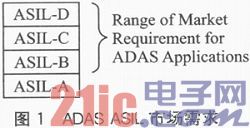
ASIL-B is the lowest level on the market, while some applications require ASIL-D to support certain features. More and more ASIL have stricter requirements. In some implementations, the generic ASIL or entry (system) level of a component introduces unnecessary complexity and has an impact on development costs and schedule. It is recommended that you understand the application requirements in detail. This is typically achieved by analyzing system concepts and drawing safety concepts and requirements from them. It is also possible to divide the application into several different steps, with different ASILs, which are easier to implement and more efficient.
ADAS single front camera application system concept
The front-end camera application in this article uses an image sensor that is common in ADAS. Figure 2 shows the overall block diagram of the system.
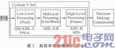
An image sensor is connected to the image processor, the Altera Cyclone V SoC. The signal processing chain and data stream are divided into 4 parts:
â—† Underlying processing at the pixel level by transforming the image into a more practical representation.
â—† Perform intermediate processing on line images or block images, and extract features such as edges using corresponding algorithms such as Sobcl filter or Canny edge detection algorithm.
â—† Perform advanced processing, extract the data of each frame, detect the target and classify it.
â—† Track the identified targets and determine if measures are needed in a hazardous environment, such as braking or shifting electronic control units (ECUs) that require communication with the microcontroller.
The low-level and intermediate-level processing can be implemented very efficiently on the FPGA, but users can also implement some intermediate-level processing on CPUs such as the Cyclone V SoC hard processor system (HPS) Cortex-A9 processor. Advanced processing is primarily control code that can be mapped to one or two Cortex-A9 in HPS. The final step in the processing chain is target tracking and decision making, which can be done on an external microcontroller.
Throughout the process, each step simplifies the input data to yield more meaningful data, and data reduction means an increase in the safety threshold. Therefore, the underlying implementation can be divided into quality management (QM) or underlying ASIL (such as ASIL-A). The reason for this is that the fault introduced during one pixel has little effect on the performance of subsequent algorithms and can be ignored. In this example, assuming that the intermediate processing is in accordance with ASIL-A or ASIL-B, the advanced processing to identify and classify the target should be in accordance with ASIL-B. After classifying the targets, a target table is generated and provided to the microcontroller for target tracking and decision making. This is the most critical part of the signal chain, and we assume that it should conform to ASIL-D, which has a direct impact on the car's ability to do so.
Component application function
Figure 3 shows the overall block diagram of an example of a single front camera system. The Cyclone V SoC is powered by an external power management circuit. A separate voltage monitoring function generates a reset when the supply voltage is not within the rated operating range. The external non-volatile memory is connected to a quad serial peripheral (quad SPI) module for loading the application and configuring FP GA during system startup. We use DDR memory when executing application code to store data and image frames. The external microcontroller is connected via SPI for target detection and final decision, and communicates with other parts of the automotive infrastructure via the CAN bus interface.
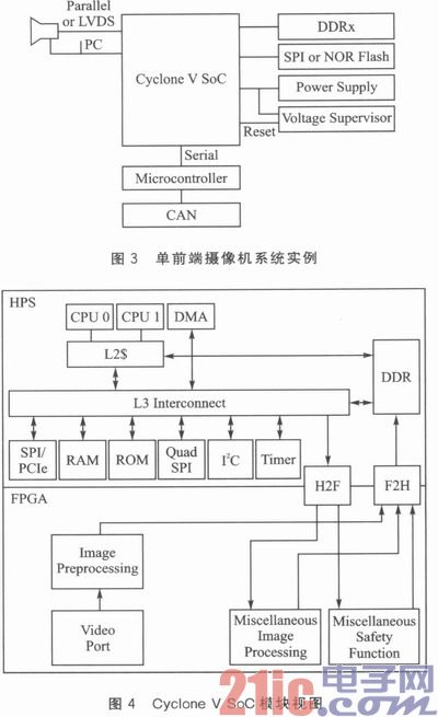
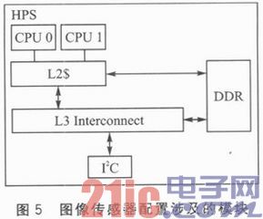
Figure 4 shows the image processor module in a single front camera application. Since the specific implementations are different, the specific implementation process of the FPGA is not described in detail, but it is sufficient for the purpose of introducing different analysis steps at a higher level of abstraction.
Image sensor configuration
Assume that the sensor is configured by the HPS system. Figure 5 shows the modules involved in the image sensor configuration. One or two Cortex-A9 CPUs execute code, and data is transferred from the DDR memory to the sensor through the I2C module. The single error correction double error detection (SECDED) error correction code (ECC) function of the DDR memory and L2 cache protects the associated memory. The parity function protects the CPU's L1 cache. This includes TAGRAM, as well as branch target access caches for global history buffers and branch prediction units. The logic associated with sensor configuration (CPU, L3 interconnect, I2C, etc.) can only be used once, without special diagnostics. To detect possible failures, write and readback methods can be used. For example, CPU0 writes configuration data to the sensor, and CPU1 reads it back. Subsequent comparisons between write data and readback data can detect faults introduced during a write session. One CPU writes data and the other CPU reads back data. This has the advantage of being able to detect permanent faults in one of the CPUs. When only one CPU is used for a write session, various software can be used to detect permanent failures. However, due to the need to perform detailed analysis of the internal functions of the CPU, the complexity of the software is increased, so this is very difficult to implement.
Some sensors used in automobiles support the transfer of certain configuration register data in the auxiliary scan lines of each image frame. With this function, you can check the sensor settings for each frame without having to read the registers through the I2C interface. No CPU overhead is required, and this check can be done in the FPGA when transferring frame data.
The advantage of all of the above configuration register tests is that it not only covers the Cyclone V SoC failure, but also the external interface of the sensor or the internal fault of the sensor. Some applications use a more complex processor architecture for internal diagnostics on the bus. However, the built-in diagnostic mechanism does not necessarily cover faults and external faults in the I2C module. These faults still need to be considered, using a mechanism similar to that discussed earlier. In this scenario, the added processor diagnostics offer limited benefits.
Underlying image processing
Figure 6 shows the modules involved in the image processing stage. In many cases, the image sensor is connected to the image processor through a parallel video interface. For Cyclone V SoC applications, the video port of the Altcra video and image processing suite can be instantiated to receive data from the sensor. These data are then passed to the image pre-processing module. After the data processing is completed, it is written to the DDR memory.
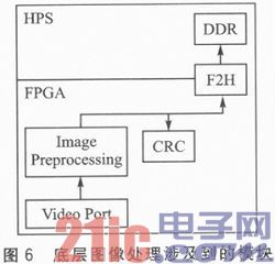
Most image sensors contain the ability to transfer defined test frames without the need to transfer normal image data. After the input data is defined, the output data of the image processing module is defined. Then carry out subsequent tests. For example, by performing a Cyclic Redundancy Check (CRC) on the output data, find any permanent faults that occur in the system. This test covers permanent failures throughout the data path. It supports testing of external connectivity issues, testing problems in video ports and image processing modules, and problems in DDR memory data transfer. Another way to check for permanent failures is to implement a test pattern generator in the FPGA fabric that can be multiplexed into the input path of the video port. The defined test pattern covers many of the faults in the entire path.
Some image sensors also have other functions such as transmitting a frame counter in each frame. This feature helps detect frame gaps, or pixel clocks, frame synchronization issues, and more. In addition, the video port implements the number of pixels per line and the line counter function. If the counter does not match the set value, an interrupt is generated. This can also be used to detect pixel clocks, as well as vertical and horizontal sync problems.
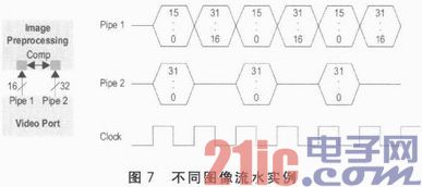
It should also detect changes in the data as a module transmits data in the FPGA. The test pattern or test frame method mentioned above covers most of the permanent faults, but no transient faults are detected. Instantaneous faults occur when implementing various image pipelines. When transferring data between modules using the Altera Avalon streaming protocol, two different interfaces may be instantiated to ensure that transient faults have different effects on data transmission in both paths. An example of different image flow is shown in Figure 7.
In many designs, you also need to use memory buffers to temporarily store data. For this case, parity or SECDEDECC can also be instantiated because the user memory in the FPGA fabric has provided the required parity for the implementation.
After the data is finally written to the DDR memory, the checksum of the data should be calculated at any time during transmission. This can be done for each frame or every row in the frame. In most cases, since the subsequent intermediate processing can read the data by row or module, it is easy to check the data, so this can be done in rows. Altera provides a CRC engine that can be instantiated in different parts of the user's design to produce a stream data CRC checksum. Adding a checksum to Niucheng's data can also cover faults that may occur in F2H bridges and DDR controllers. The data in the DDR is then protected by the SECDED ECC and the checksum. Another fault that needs to be considered is that the data address may change. To avoid overwriting other critical application data, the DDR memory controller implements a memory protection function that defines 20 different memory areas with different access rights and the host can access certain areas.
Intermediate image processing
Viewing only the features of interest in the image reduces the amount of generated data. After the data is reduced, the risk of losing features increases and the risk of errors in the application increases because the failure causes the target to be lost in subsequent processing steps. Figure 8 shows the modules involved in intermediate level image processing.
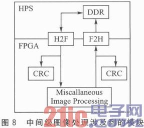
It is necessary to read back the data generated by the previous image preprocessing stage and the data stored in the external DDR memory for various image processing. Since the previous data is appended with a CRC checksum, it can be checked again to see if the data was modified during the external memory or if it was modified when transferred to the FPGA.
It is best to implement some memory buffering at this processing level to temporarily store the data. A relatively high diagnostic coverage can be achieved by instantiating parity or SECDED ECC for these memories again.
Detecting the failure of the logic itself, you can put two identical logic modules together and lock them. To be able to detect common faults, you can use a different clock network for them or run a logic module with a two-cycle clock delay. Continuous comparison of the outputs of the two modules enables detection of faults in one module.
After this intermediate processing stage has generated new data, it needs to be written to the external DDR memory again. As with the previous steps, a checksum can be calculated for the new data and written to the memory. The memory protection feature in the DDR memory controller detects address failures and avoids overwriting other critical application data.
Advanced image processing
The advanced image processing stage includes target detection and target classification. From a software terminology perspective, this level is primarily control code and, therefore, is ideal for running on a CPU. In our application examples, such features can be developed in HPS. Figure 9 shows the modules involved in advanced image processing.
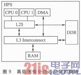
Although two CPUs are implemented, they are not running in lock mode, that is, one CPU checks and the other automatically detects faults during program execution. If a CPU that executes safety critical code or data fails, the application should ensure that the results of the calculation are checked. This can be done by redundantly executing code on the same CPU or another CPU. If a CPU has a permanent failure and the same code is executed twice on one CPU, the failure in the CPU may result in two errors and will not be detected. This problem can be avoided by implementing two different programs, but the disadvantage is that it increases the development effort and develops two different versions for the same program. Another option is to run redundant calculations on the second CPU. A permanent failure in one CPU does not affect the other CPU, so as long as the failure is not in a shared resource, error execution can be detected without running different software. Run the algorithm twice and then compare the results to detect transient faults. In the case where the software is executed on two CPUs, it is likely that the same code is not executed in the same cycle of both CPUs, so the calculation can be performed and then the output of the redundant execution can be compared to find the fault. The advantage of executing code at different times is that it can effectively detect common faults.
As mentioned earlier, the memory involved in the process is protected by the SECDED ECC or parity function.
Failures may occur in other logics such as L3 interconnects, DDR memory controllers, and on-chip RAM controllers. For larger data, a CRC checksum can be used to protect the data from being modified. After the checksum is established for the data generated by the intermediate processing module, it can be checked before being used for subsequent operations. For smaller data, store the data and read back to determine if the transfer is correct. For reading data for processing, you can read it twice and compare it before use. This does not incur too much processing overhead when the data size is limited, but it can detect faults well.
Other features for detecting faults include the Memory Management Unit (MMU) in each Cortex-A9 processor, the memory protection features in the DDR memory controller, and the watchdog timer.
in conclusion
ADAS is the next wave of innovations to ensure a safer and more crowded road. The performance requirements of these systems present challenges to existing and future standard commercial shelf (COTS) products, and programmable FPGAs have significant advantages in this regard. Special diagnostic functions such as custom pattern generators or custom watchdog timers can improve the diagnostic coverage of the system, which is difficult to implement on standard products. Stream processing is the first step in image processing, reducing memory read and write operations, thus reducing the occurrence of faults, reducing power consumption, and improving application performance. Many COTS products are not designed to be functionally safe. Using a functionally safe platform and development environment, and working with partners who are good at functional safety, are conducive to the overall implementation of the system.
Electric Spiral Stove,Cooking Plate Stove,Electric Cook Stove,Spiral Hot Plate Electric Stove
Shaoxing Haoda Electrical Appliance Co.,Ltd , https://www.hotplates.nl