MC3359 DATASHEET MC3359 is a single-chip narrow-band FM receiver circuit produced by American MOTOROLA company, which is mainly used in wireless receivers for voice communication. The chip contains an oscillating circuit, mixing circuit, limiting amplifier, AFC (automatic frequency control), integral discriminator, filter, suppressor, scanning controller and noise suppression switch circuit. The MC3359 is similar to the MC3357, and adds a mid-amplifier limiting amplifier stage, an AFC output stage, and a FM detector on the basis of it. It is mainly used in the second frequency conversion communication receiving equipment using a 455kHz ceramic filter. The MC3359 also requires fewer external components. The operating voltage is required to be below 6.0V, which is suitable for economic applications. MC3361BP and BD are recommended. If a fixed frequency point of a ceramic filter is used, similar double-conversion receiving circuits can refer to MC3335, MC3362, MC3363. The main characteristics of MC3359 are as follows: 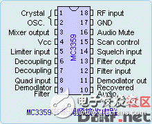 · Low power consumption (at Vcc = 6.0V, the typical power consumption is only 3.6mA) · Low power consumption (at Vcc = 6.0V, the typical power consumption is only 3.6mA) · Limit sensitivity: 2.0uV (-3bB) (typical value) · A small number of external components · DIP18 and SO-18 packages · If low voltage and RSSI are required, it is recommended to use the MC3371 receiver circuit with better performance  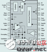 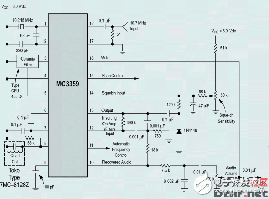 The internal oscillation circuit of MC3359 and the external components of Pin1 and Pin2 form the second local oscillator stage. The first intermediate frequency IF input signal 10.7MHz is input from Pin18 of MC3359, and is mixed at the internal second mixing stage. The difference frequency is 10.700. -10.245 = 0.455MHz, that is, 455kHz second intermediate frequency signal. The second intermediate frequency signal is output by Pin3, the frequency is selected by a 455kHz ceramic filter, and then sent to the limiting amplifier of MC3359 via Pin5 for high gain amplification. The limiting amplifier stage is the main gain stage of the entire circuit. The external components of Pin8 form a 455kHz frequency-resonant resonant circuit. The amplified second intermediate frequency signal is internally frequency-decoded and demodulated, and the audio signal is output by Pin10 after being amplified by the first-level audio voltage. Pin14——Pin17 is the carrier frequency detection and electronic switch circuit. The carrier frequency detection circuit can be formed by connecting a small number of components for the noise control of the FM receiver. There is also a first-stage filter signal amplification stage inside the MC3359. A small number of external components can form an active frequency selection circuit to provide signals for the carrier frequency detection circuit. The filter Pin12 is the input terminal and Pin13 is the output terminal. Pin6, Pin7 and Pin9 are the decoupling capacitors of the second intermediate amplifier. MC3359 limit parameter (Ta = 25 ℃) name pin position identifier limit value unit power supply voltage 4Vcc (max) 12V (DC) working voltage range 4Vcc6-9V (DC) input voltage 18V181.0VRSM squelch function 16V16-0.7— 12Vpk welding temperature-Tj150 ℃ working ambient temperature range-TA-30— + 70 ℃ storage temperature-Tstg-65— + 150 ℃
|
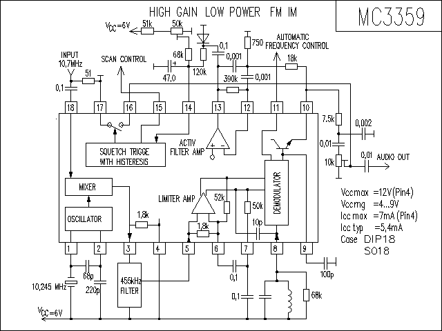
Working principle of MC3359 narrow-band FM receiving circuit:
The internal oscillation circuit of the MC3359 and the external components of Pin1 and Pin2 form the second local oscillator stage. The first intermediate frequency IF input signal 10.7MHz is input from the Pin18 of the MC3359, and is mixed at the internal second mixing stage. -10.245 = 0.455MHz, that is, 455kHz second intermediate frequency signal.
The second intermediate frequency signal is output by Pin3, the frequency is selected by a 455kHz ceramic filter, and then sent to the limiting amplifier of MC3359 via Pin5 for high gain amplification. The limiting amplifier stage is the main gain stage of the entire circuit. The external components of Pin8 form a 455kHz frequency-resonant resonant circuit. The amplified second intermediate frequency signal is internally frequency-decoded and demodulated, and the audio signal is output by Pin10 after being amplified by the first-level audio voltage.
Pin14——Pin17 is the carrier frequency detection and electronic switch circuit. The carrier frequency detection circuit can be formed by connecting a small number of components for the noise control of the FM receiver. There is also a first-stage filter signal amplification stage inside the MC3359. A small number of external components can form an active frequency selection circuit to provide signals for the carrier frequency detection circuit. The filter Pin12 is the input terminal and Pin13 is the output terminal. Pin6, Pin7 and Pin9 are the decoupling capacitors of the second intermediate amplifier
| Limit parameters of MC3359 (Ta = 25 ℃) | |||||
| name | Pin location | Identifier | Limit value | unit | |
| voltage | 4 | Vcc (max) | 12 | V (DC) | |
| Working voltage range | 4 | Vcc | 6-9 | V (DC) | |
| Input voltage | 18 | V18 | 1.0 | VRSM | |
| Squelch function | 16 | V16 | -0.7—12 | Vpk | |
| Welding temperature | - | Tj | 150 | ℃ | |
| Working ambient temperature range | - | TA | -30— + 70 | ℃ | |
| stored temperature | - | Tstg | -65— + 150 | ℃ | |
MC3359 receiving circuit
High Speed Blender,Powerful Blender,High Power Blender,Multi Function Blender
Shaoxing Haoda Electrical Appliance Co.,Ltd , https://www.hotplates.nl