This article designs the network storage on the 1553B bus. The entire system is designed based on the NIOS II core, using SoPC technology to integrate the logic control of the interface part into the FPGA chip, and the storage capacity and the number of nodes of the system can be expanded.
The 1553B bus, which was born in the 1970s, is a master-slave redundant bus. It has strict regulations on bus hardware, and has good reliability and real-time performance. It has become the first choice for military electronic buses today. Similar to Ethernet, 1553B networking also has storage requirements such as "network hard drives" to alleviate local storage pressure and can be used as data relays for other parts and even other networking.
The Nios II embedded processor is the second-generation configurable soft-core processor for programmable logic devices introduced by Altera in June 2004. Its performance exceeds 200 DMIPS. Nios II is a RISC universal embedded processor soft core based on Harvard architecture, which can be combined with user logic and programmed into Altera's FPGA. The processor has a 32-bit instruction set, 32-bit data channel and configurable instructions and data buffer. It is optimized for programmable logic, and also designed a comprehensive solution for programmable single-chip system (SoPC).
Overall system plan
The main function of this system is to receive commands and data from the 1553B network, manage the back-end storage, and provide a network interface to access the storage. The memory interface of the system serves as a slave node in the 1553B bus, which is usually in a standby state. When a read and write command is sent on the bus, the bus conversion interface reads data from or writes data to the post-level memory according to the command. For the bus protocol, the most convenient is to use off-the-shelf protocol chips, but the cost of doing so is very high. The single-chip price of the 1553B protocol chip is more than 6000 yuan, which is a big burden for ordinary applications. FPGA protocol management will greatly reduce the cost. In addition, Quartus contains a lot of memory management IP cores for use. For the 1553B protocol, you need to customize the components yourself.
The system program consists of two parts, one is to receive network commands and data, and the other is to read and write memory. In the NIOS IDE environment, C language is used as the programming language.
System hardware design
The hardware block diagram of the system is shown in Figure 1.
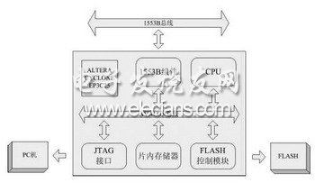
Figure 1 Block diagram of system hardware structure
The core chip of the system adopts Altera's CYCLONE III series FPGA EP3C25F324. It uses 65nm low-power process technology for production. Its integration and performance have been significantly improved, but the power consumption is very low. In addition, the CYCLONE series has always been positioned as a low-cost device.
With the SOPC software integrated in Quartus II 7.2, the Nios II core is transplanted to the FPGA. The required components are as follows.
CPU: Select the standard CPU core, and the Debugger is Level 1, and try to save the use of on-chip resources when the demand is met.
System_ID: Used for system authentication when downloading.
Jtag_uart: The communication interface between FPGA and PC, it will be very convenient to use in NIOS IDE software.
onchip_memory: On-chip memory, used when transferring data.
FLASH: The Quartus software internally integrates the 128P308 control component produced by Intel Corporation, which is easy to develop. If a larger amount of storage is required, increase the FLASH capacity. If necessary, you can hang a few more.
FLASH_Bus: FLASH data is three-state, need to add Avalon three-state bus bridge between CPU and FLASH.
1553B interface component: It is the interface for communicating with the external 1553B bus. The component is not integrated in the Quartus software and needs to be developed by itself.
On the 1553B network, this system is designed as a slave node. Inside the system, the interface component of 1553B needs to be the master port on the Alavon bus, and the remaining memory control modules as slave ports. Since the remaining ports are integrated within the Quartus software, the main workload of system software design is component development of the 1553B interface.
The memory chip adopts the FLASH chip of 128P308 produced by Intel, which conforms to the general interface standard, which is convenient for the subsequent update of the functional capacity.
System software design
The core task of customizing 1553B components is to convert the 1553B bus signal to the Avalon bus inside NIOS II.
The 1553B component serves as the main port on the Avalon bus, and the selected signals include clk, address, read, write, data, irq, reset, and irqnumber. The transmission mode is the basic main port read transmission and write transmission. The generation of these signals requires the frame signals read from the 1553B bus. There are three frames on the 1553B bus, command frame, status frame and data frame. The structure of these three frames is shown in Figure 2.
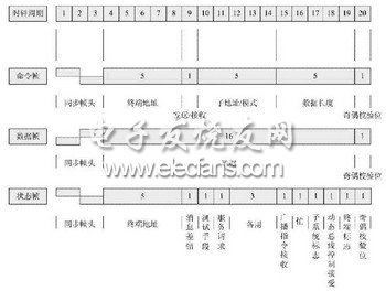
Figure 2 Three frame structures of 1553B bus
For these three frames, the command frame, data frame and status frame can use the same buffer, because the slave node as the storage will not actively send data to the master node, the entire work is passively receiving the master node's command, waiting The main node reads or writes data, and the system has only a single state without conflicts.
For the signals in the Avalon bus, the corresponding signal relationships within the frame are as follows.
read / write signal: the send / receive bit in the command frame.
address signal: The sub-address and data length bits in the command frame.
data signal: data bits in the data frame.
irq signal: caused by the flag bit in the status frame.
irqnumber signal: the specific position within the status frame.
The API functions of the 1553B component include:
altera_avalon_1553B_init ()
altera_avalon_1553B_enable ()
altera_avalon_1553B_disable ()
altera_avalon_1553B_getframe ()
altera_avalon_1553B_sendframe ()
The rest of the steps for customizing components are not repeated here. After the component is defined by SoPC, it is named 1553B and added to the NIOS II core.
Mid Light designed LED Wall Clock with night light.
Battery operated or electricity driven clock, with wall light for wall decorations.
With metal, bamboo, mirror and wooden material for selection, with green, red, yellow, white and blue Light Clock hand.
The colorful clock hand will light up at night, a special Wall Art Decor for your home, office or bar.
But this wall decor is for interior decoration only, not suitable for outdoor use.
Decorate your home with this wall light with time, you'll be suprised.
Lighting Wall Clock,Light Up Wall Clock,Lighted Wall Clock,Mid Light Wall Light
Guangzhou Huanyu Clocking Technologies Co., Ltd. , https://www.findclock.com