This article briefly introduces the Link Training and Status State Machine (LTSSM) and briefly introduces the role and implementation mechanism of each state.
LTSSM has 11 states (including multiple sub-states) Detect, Polling, Configuration, Recovery, L0, L0s, L1, and L2 (L3 is optional), Hot Reset, Loopback, and Disable. After the system performs a reset operation (Cold, Hot or Warm Reset), it automatically enters the Detect state.
These 11 states can be further divided into the following five categories:
1, Link Training State (Link Training State);
2, Re-Training (Recovery) State;
3, Software Driven Power Management State (Software Driven Power Management State);
4. Active-State Power Management State (ASPM State);
5, Other State (Other State);
As shown below:

Here's a brief overview of each state:
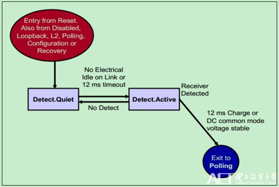
The first is Detect:
As mentioned earlier, after the system performs a reset operation (Cold, Hot or Warm Reset), it will automatically enter the Detect state. In this state, the PCIe device will detect if there is another PCIe device at the other end of the Link. In other words, it is to detect if there are other PCIe devices connected to it. As shown below:
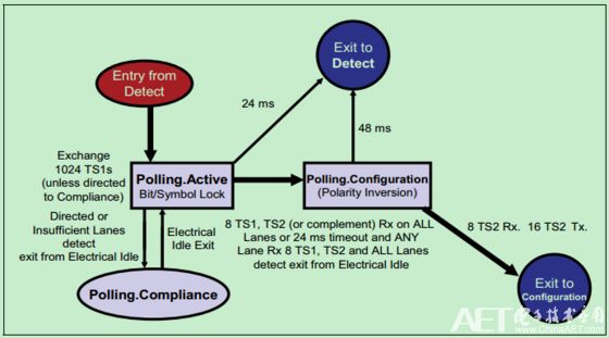
Polling:
In this state, the PCIe device sends TS1OS and TS2OS in turn to achieve the following goals:
1, Bit lock (Bit Lock);
2, the character lock (Symbol Lock);
3, Polarity Inversion (Polarity Inversion), if needed;
4. Determine the data rates supported by each device.
As shown below:
Configuration:
In this state, the PCIe device sends TS1OS and TS2OS in turn to achieve the following goals:
1, determine the link width (Link Width);
2, the distribution channel (Lane) number;
3, Lane Reversal (Lane Reversal), if needed;
4. Lane-to-Lane De-skew.
As shown below:

L0:
This is the Normal and Full-Active State of the Link. All TLPs, DLLPs, and Ordered Sets can be sent and received normally. In this state, the rate can be 2.5 GT/s or 5 GT/s (if both ends of the link are supported and Re-Trainning).
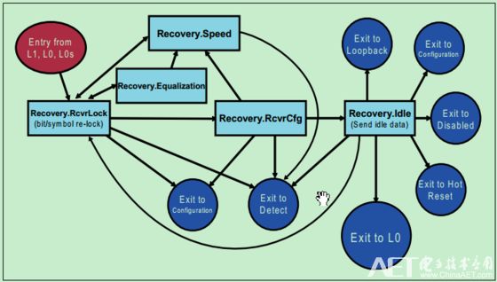
Recovery:
This state is used for Re-Trainning, so Re-Trainning may change the original rate, so Bit Lock and Symbol Lock operations will be re-executed, but it will take less time than the first time. a lot of.
Its internal substate transition diagram is shown below:
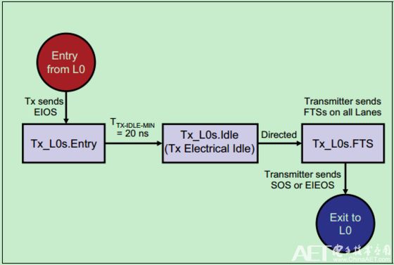
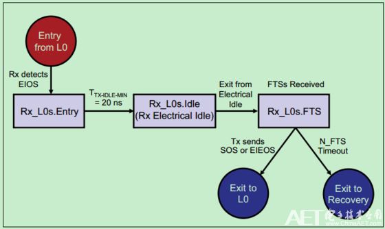
L0s:
The ASPM state is mainly used to reduce power consumption, and can enter this state when the bus is idle, and from this state can quickly switch back to the L0 state again. When the L0 state is, EIOS appears on the link, indicating that the L0s state is about to enter. When in the L0s state, FTS occurs on the link, the link will quickly complete bit lock and symbol lock, and enter the L0 state.
The sending end is shown in the figure below:
The schematic diagram of the receiving end is as follows:
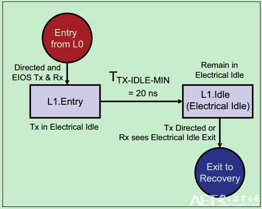
L1:
Relative to the L0s state, the power consumption in the L1 state is lower. Entering the L1 state requires "communication" between the PCIe at both ends of the link. Only when both parties "agree" to enter this state, the link will enter this state. There are generally two ways:
1. The first one is booted by ASPM and the hardware automates it. When the sender discovers that there is no TLP or DLLP on the link for a long time, it recommends that the receiver enter the L1 state through the ASPM. If the receiver "agrees", the link enters the L1 state; if the receiver "disagrees," the link enters the L0s state.
2. The second type is software-directed. The software sends a series of commands to put the link into a low-power state (D1, D2, or D3 Hot). Subsequently, the upper device of the link will notify the lower device to enter the L1 state. After receiving the response from the lower device, the link enters the L1 state.
As shown below:
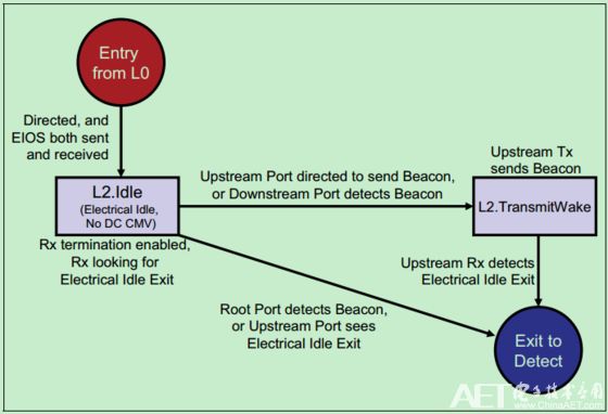
L2:
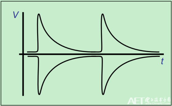
The link power consumption in the L2 state is lower because it only retains Vaux and shuts down the other functions of the link. At this point, the Beacon signal or WAKE# sideband signal is needed to wake up the system. The Beacon signal is a low-frequency signal (30KHz~500MHz). The waveforms are as shown in the figure below:
Note: In addition, there is an L3 state, but it is not actually LTSSM. Since the L3 state is closed even when Vaux is turned on, once it enters the L3 state, there is actually not much difference between the power supply and the power of the PCIe device.
The substate transition diagram of L2 is shown in the figure below:
Loopback:
This state is mainly used for testing, not described in detail here.
Disable:
In this state, the link is disabled. At this time, the sending end is in an Electrical Idle State and the receiving end is in a Low Impedance State. The reason for entering this state may be that the link connection is unstable or a device in the link is removed, such as a PCIe card being pulled out of the slot.
Hot Reset:
Software can reset the link by setting the Secondary Bus Reset bit in the Bridge Control Register. Subsequently, the PCIe device at the bottom of the bridge sends the TS1OS, and the Training Control contains the Hot Reset information. When the receiver finds that Hot Reset is included in both consecutive TS1OS, the link then enters the reset state.
Note: This article is just a brief introduction to LTSSM. For how to implement each specific state, please refer to PCIe Spec related chapters.
Ceramic Switch,Ceramic Light Switch,Ceramic Rotary Switch,Alumina Ceramic Switch Block
Yixing Guangming Special Ceramics Co.,Ltd , https://www.yxgmtc.com