0 Preface
With the development of electronic technology and wireless communication technology, people's pursuit of living standards is getting higher and higher. Intelligentization is well known. As one of the intelligent intelligent lighting systems, it has a good development prospect in the field of future lighting. Most of the traditional lighting systems use wired connections, which are troublesome to lay, expensive, difficult to expand, complicated to install, difficult to move and maintain, and high in energy consumption. In view of the deficiencies of traditional lighting, wireless data transmission can be used instead of wired transmission. ZigBee technology is a new type of wireless communication technology with unified technology standards. It is applied to low-rate transmission in short range. It has low power consumption, low cost, reliable data transmission and large network capacity. It is very suitable for lighting systems. use. In addition, the rapid development of the IC industry can be utilized, and efficient and low-energy driving technologies can be used to reduce lighting costs, thereby achieving energy saving and emission reduction. This paper introduces a scheme to realize remote control of LED energy-saving lamps by using ZigBee wireless sensor network technology, and gives detailed hardware and software design.
1Self-network control system and working principle
In order to realize fault detection, temperature detection, voltage detection, brightness detection and control, and fault alarm, the self-organizing network control system adopts the design shown in Figure 1.
The entire wireless network is composed of three devices: a ZigBee Endpoint (ZE), a ZigBee Router (ZR), and a ZigBee Coordinator (ZC). The terminal is a Reduced Function Device (RFD), which can only communicate directly with the router or the coordinator. Routing is a Full Function Device (FFD) that communicates directly with routes and terminals, as well as with the coordinator. The coordinator is the PAN Coordinator (PANC), which is responsible for network establishment and management of a PAN area. The coordinator collects information about all nodes and routes and sends them to the monitoring computer via RS232 to determine the brightness of the lamp, the ambient temperature, the battery level, and so on.
Working principle: Each terminal and route in the system respectively control one light. Each light corresponds to an ID (the terminal or route is automatically assigned by the coordinator when joining the network), and each node and route sends the data collected by the sensor to the coordination by wireless. The coordinator sends the received data to the monitoring computer through the serial port. If the LED light fails, the detection circuit will generate an alarm signal, and the alarm signal will eventually be sent to the monitoring computer. The computer will prompt the staff to indicate the ID of the fault light, which makes the maintenance more convenient. In addition, the terminal's light sensor collects the degree of illumination, and then the terminal automatically adjusts the brightness of the light. The terminal also transmits its own supply voltage to the monitoring computer to prevent the node from running out of power.
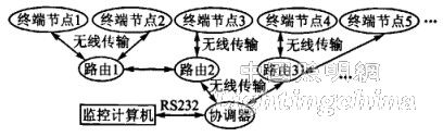
Figure 1 System design diagram
2 system hardware design
The system is composed of power module, wireless transmission module (CC2530, temperature detection, voltage detection), LED driver module, LED detection module, etc. The logic structure of the specific hardware circuit is shown in Figure 2. The power module is based on the commonly used ASMlll7-5.0 and ASMlll7-3.3, and the principle is simple and easy to understand. The following mainly introduces the wireless communication module and the LED driver module.
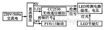
Figure 2 logical structure block diagram of the hardware circuit
The wireless communication module uses TI's CC2530 module, a true system-on-a-chip (SoC) solution for IEEE 802.15.4, ZigBee and RF4CE applications. It is capable of building powerful network nodes at very low total material costs. The CC2530 combines the performance of leading RF transceivers with an industry-standard enhanced 8051 CPU, in-system programmable flash, 8 KB RAM and many other powerful features. The CC2530 is available in four different flash versions: CC2530F32/64/128/256 (32/64/128/256 KB flash respectively). The CC2530 has different operating modes, making it especially suitable for systems with ultra-low power requirements. The short transition time between operating modes further ensures low energy consumption.
CC2530's excellent performance and low power consumption with code prefetch, 8051 microcontroller core, 32/64/128 KB in-system programmable flash, 8 KBRAM, data retention and support in various power modes Hardware debugging, with high receiving sensitivity and anti-interference performance. It has a programmable output power of up to 4.5 dBm and requires very few external components. The block diagram of the hardware circuit is shown in Figure 3. The light control unit uses the TPS851 chip and the temperature control module uses the TC77.
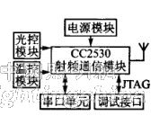
Figure 3 node hardware circuit logic diagram
The chip used in the LED driver module is the PT4115. The PT4115 is a continuous inductor current conduction mode buck constant current source for driving one or more series LEDs. The PT4115 has an input voltage range of 6 to 30 V and an adjustable output current of up to 1.2A. Depending on the input voltage and external components, the PT4115 can drive LEDs up to tens of watts. Within PT4115
Set the power switch, use high-side current sampling to set the average LED current, and accept analog dimming and a wide range of PWM dimming through the DIM pin. When the voltage of the DIM is lower than 0.3 V, the power switch is turned off, and the PT4115 enters a standby state with extremely low operating current. The driving principle diagram is shown in Figure 4. PT4115 and inductor L, current sampling resistor RS form a self-oscillating continuous inductor current mode buck, constant current LED controller. When VIN is powered up, the initial currents of L and RS are zero, and the LED output current is also zero. At this time, the output of the CS comparator is high, the internal power switch is turned on, and the potential of the SW is low. The current flows from VIN to ground through L, RS, LED and internal power switch. The slope of current rise is determined by the voltage drop of VIN, L and LED. A voltage difference Vcsn is generated on RS. When Vin-Vcsn>115mV, CS comparison The output of the device goes low, the internal power switch is turned off, and the current flows through the L, RS, LED, and Schottky diode (D) with another slope. When Vin-Vcsn <85 mV, the power switch is turned back on, so that The average current on the LED is loI = (0.085 + 0.115) / (2 x Rs) - 0.1 / Rs.
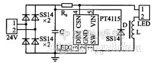
Figure 4 LED drive schematic