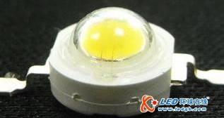
The LED package is formed by a die (die) through a wire bonding, eutectic or flip chip packaging technology and a heat sink substrate Submount (sub-adhesive technology) to form an LED chip, and then the chip is fixed on the system board and linked into a light source module.
At present, the LED packaging method can be roughly divided into a lens type (Lens-type) and a reflector type (Reflector-type), wherein the lens can be formed by molding or lens bonding; as shown in FIG. 1(a) The reflective cup chip is mostly formed by mixing, clicking, and packaging; as shown in Figure 1(b).

In recent years, epitaxial, solid crystal and package design have gradually matured. The grain size and structure of LEDs have been miniaturized year by year. The power of single crystals of high power is 1~3W, even more than 3W. When the LED power is continuously improved, for LED crystal The heat dissipation and heat resistance requirements of the particle-borne version and the system circuit board are becoming increasingly stringent.
In view of the comprehensive considerations of insulation, pressure resistance, heat dissipation and heat resistance, ceramic substrates have become one of the important materials for the secondary adhesion technology. The technology can be divided into a thick film process (Thick film), a low temperature co-firing process (LTCC) and a thin film process (DPC). However, the thick film process and the low-temperature co-firing process use screen printing technology and high-temperature process sintering, which is prone to rough lines, inaccurate alignment, and shrinkage ratio. If the line is more and more sophisticated, high-power LED products, For LED products that require accurate eutectic or flip chip processes, thick-film and low-temperature co-fired ceramic substrates are gradually in use.
For this reason, the high heat dissipation coefficient thin film ceramic heat dissipation substrate is formed by sputtering, electric/chemical deposition, and yellow light lithography process, and has the characteristics of precise metal lines and stable material system, and is suitable for high power, small size, high brightness LEDs. The development trend has solved the stringent requirements for the resolution and accuracy of the metal substrate of the ceramic substrate in the eutectic/wrapping process. The thin film ceramic COB (Chip On Board) heat sink substrate can meet different lighting needs.
When the LED die is made of ceramic as the carrier, the heat dissipation bottleneck of the LED module is transferred to the system circuit board, which transfers the heat energy from the LED chip to the heat sink fin and the atmosphere. As the function of the LED die is gradually improved, the material It has also gradually changed from FR4 to metal core printed circuit board (MCPCB), but with the development of high-power LEDs, the thermal coefficient of MCPCB material (2~4W/mk) cannot be used for higher power products. For this reason, ceramics The demand for a circuit board has become increasingly popular.
In order to ensure the material stability and light decay stability of LED products under high power operation, the trend of using ceramics as heat dissipation and metal wiring substrates has become increasingly clear. Ceramic materials currently cost more than MCPCB. Therefore, how to use the high heat dissipation coefficient of ceramics to save material use area to reduce production costs has become an important indicator for the development of ceramic LEDs. Therefore, in recent years, the integration of polycrystalline packages and system lines with ceramic material COB design has gradually attracted the attention of various packaging and system manufacturers.
COB is not a new technology in the electronics manufacturing industry. It refers to directly bonding bare wafers to the circuit board and soldering the wires/solder wires directly to the gold-plated lines of the PCB. It is also known as Wire bonding. And through the sealing technology, the packaging steps in the IC manufacturing process are effectively assembled directly on the circuit board. In the LED industry, as modern technology products become more and more lightweight and highly portable, in addition, in order to save the system board space problem of multiple LED chip design, in the demand of high-power LED system, the direct development of the die COB technology adhered to the system board.
The advantages of COB are: high cost efficiency, simple circuit design, saving system board space, etc., but there are also technical thresholds for integrated brightness, color temperature adjustment and system integration. Taking a 25W LED as an example, a traditional high-power 25W LED light source must be packaged into 25 LED components using 25 1W LED chips, while the COB package is to package 25 1W LED chips in a single chip. The secondary optical lens will be reduced from 25 to 1 piece, which will help to reduce the light source area, reduce material, and system cost, thereby simplifying the secondary optical design of the light source and saving assembly labor costs.
In addition, the high-power COB package requires only a single high-power LED to replace multiple LED packages of 1 watt or more, which makes the product thinner and lighter. At present, COB products are still mainly used in the production of COPCB products. However, MCPCB still has many problems of heat dissipation and excessive light source area, so the fundamental way is to update from the heat dissipation material to the most effective solution.
The ceramic COB substrate has the following advantages: 1. The thin film process makes the basic circuit more precise; (2) The large amount reduces the cost; (3) The plasticity is high, and can be done according to the different needs of the partners.
The development of COB is to simplify the trend of system boards. The practical use of lighting fixtures, brightness, heat dissipation and cost control are all important factors. In addition to providing a variety of thin film heat sink substrates for single chip packaging, ICP also provides an independently developed thin film line COB substrate, which is a more flexible choice for users of different high power applications, in the hope that LED lighting will become more popular as soon as possible. To make a contribution to the greening of the earth.
32mm DC Spur Gear Motor is mainly including 32RS385 and 32RS395 two types.
Differed with 33Mm Dc Spur Gear Motor or 37mm DC Spur Gear Motor, 32Mm Dc Spur Gear Motor has a center shaft.

32mm Dc Spur Gear Motor has 6 stages.
For the 2 stages gearbox, we have 5.75 gear ratio;
For the 3 stages gearbox, we have 13 and 15 gear ratios;
For the 4 stages gearbox, we have 28, 32, 38 gear ratios;
For the 5 stages gearbox, we have 61, 71, 82, 96 gear ratios;
For the 6 stages gearbox, we have 135, 156, 181, 211, 245 gear ratios;
For the 7 stages gearbox, we have 196, 344, 400, 464, 540, 627 gear ratios
| Number of stages | 2 | 3 | 4 | 5 | 6 | 7 |
| Reduction Ratio | 5.75 | 13, 15 |
28, 32 .38 |
61, 71, 82, 96 |
135, 156, 181, 211, 245 |
296, 344, 400, 464, 540, 627 |
| Gearbox Length(L) mm | 17.5 | 20 | 22.5 | 25 | 27.5 | 30 |
| Breaking Torque(kg f.cm) | 8 | 10 | 15 | 20 | 24 | 24 |
| Gearbox efficiency | 81% | 73% | 65% | 59% | 53% | 48% |
32mm DC Spur Gear Motor
32Mm Dc Spur Gear Motor,32Mm Gear Motor,32Mm Dc Gear Motor,32Mm Planetary Gear
SHENZHEN DONGMING MOTOR CO., LTD. , http://www.dongminggp.com