In a bright sunny day, I am planning a circuit module to be designed. What needs to be done this time is a high precision, high load regulation LDO with large off-chip capacitors to power the low-voltage part of the entire chip. LDO's IP is just coming from his colleague, Kiang. It uses the structure of Miller compensation. Although this is a very reliable colleague, although it seems that there are some more clever places to do, the heart can not help but be puzzled: Is Miller compensation really sufficient for such a large output capacitor? The seeds of this question actually took root as early as a month ago. The beginning of the complete story is this, once made by a DAC controlled by the Buffer, positive and negative high voltage ClassAB output with a large 10uF capacitor, under normal circumstances no load, output level adjustment or switch need to be relatively large SR, then when the output current returns within the current limit value, it can be considered that the process of Settling is started (the output no longer limits the current indicating that gm has exited the saturation state). At this time, the load current will still change from a relatively large value to an empty load. The process requires Buffer stability. Considering that the output has a 10uF capacitor, and under most circumstances no-load, the output frequency of the output pole will be as low as about 0.03Hz, and there will also be a process of changing the load current. Therefore, it may be difficult to use Miller compensation and consider The overhead to the high voltage capacitor would be very large, so at that time it was decided to use the most generous compensation method (in the moment of knocking off this paragraph, I suddenly thought that in fact, the voltage divider and the source follower combination can be used to connect both ends of the Miller capacitor On the low voltage field, one can't help but feel that old blood is going to spit out. It was so amateur.
Just before someone just asked why this circuit does not use Miller compensation? What is the difference between the application of this circuit and LDO? Although Balla Ballaba talked about the above considerations again, in fact, the small emotions that I have had in my mind have fluctuate: Yes, why can't I use Miller compensation? Many times when it comes to LDOs with off-chip large capacitors, as a person who has never done anything before, the first impression in the mind always comes up with those "ESR fixed zero", "zero pole tracking", etc. Nouns, even without careful scrutiny, "deny by feeling" the possibility of Miller compensation. In fact, after finding some papers and looking at it recently, it was discovered that there were a lot of design methods and cases based on Miller compensation in the LDO field, and it was still too few to read their own books! However, it is a coincidence that the above problem has been carefully scrutinized due to an incorrect simulation of the previous days, and the Miller effect and compensation have been re-examined in a way that is as simple and intuitive as possible. Now I have included it. The lessons of simulation mistakes and some divergent thoughts are shared. Of course, it is possible to understand the correct and possibly give wrong explanations. The reason why they should be written cheeky, the power is to hope that they can give you a few ideas and make a little difference. Small contribution!
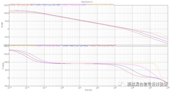
figure 1
Well, the end of the foreplay, the start of the film: After getting the IP of a colleague, I understand all the truth, so people don't talk much and go straight! But after running the stb simulation, as shown in Figure 1, when a single pole gain curve lying in a slightly perfect unity gain bandwidth lays in front of you, in fact, my entire body is uneasy, originally at the extremely low frequency output pole. Can it really be pushed out of unit gain bandwidth at once, even when it is almost empty? Do you think the loop breakpoint is set wrong? Always set the loop breakpoint at the high resistance point of the FB, but this time it is not confident, so we changed the breakpoint to the output and got the simulation result shown in Figure 2. Under such breakpoint conditions, the simulation finds that the main pole position energy coincides with the output pole, but sees a more recent zero and second pole. So once again fell into a deep doubt: the secondary pole is because the load capacitance is too large and Miller compensation invalidated at the feedback node of the pole? What is the ghost of this zero point? Because this Miller compensation uses the Ahuja connection to the cascode source of the first-level op amp folding point, as shown in Figure 3, the first reaction is whether there is any hidden bug in this connection, such as the folding point below. The output impedance of the current source drain decreases.
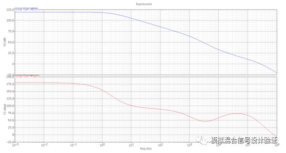
figure 2
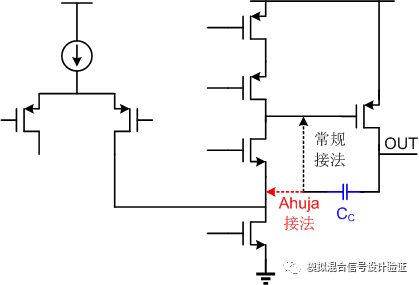
image 3
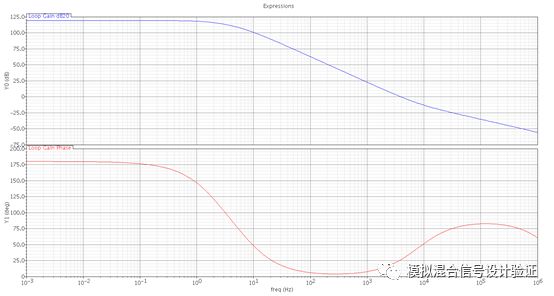
Figure 4
Then try to replace the Ahuja connection method with a conventional connection. After simulating stb, we found that there are two very close poles in the low frequency. As shown in Figure 4, one frequency is consistent with the output pole, and the other looks like the Miller effect. The resulting pole, at one point, thought that Ahuja's connection invalidated Miller compensation for some reason. Helped some friends in the IC group, and the answers given by everyone did not fully explain the doubts. So I discussed the above-mentioned simulated phenomenon with my colleagues. At the beginning, he was very aggressive when he saw the waveform, or he was led by my preconceptions. Two days later, the colleague found a breakthrough point. He used AC to perform closed loop simulation. The bandwidth position can be matched with Miller compensation bandwidth. So, after having in-depth exchanges with the analog design people's old friends - Paper, books and the other half of the brain, the problem was found: 1. The loop breakpoint was indeed set wrong; 2. Miller compensation in this There is no failure under the load capacitance; 3. The output pole is pushed further by the Miller compensation.
This conclusion is actually very simple. Maybe you would say that you have made a mistake and you have made a mistake. However, these days I carefully reviewed the entire process of the development of the problem. I think that the reason for making such a mistake is, in fact, not being able to master the arts and failing to fully understand the principles of Miller effect and Miller compensation! We are often good at remembering some simple conclusions without actually asking “why†and then dig more. Returning to the three points in the conclusion, for the first question, we may all have such experience. If the position of the loop is not correct, some abnormal results will often appear. However, it is not clear exactly where it is broken. It is wrong and why it is wrong, so for insurance reasons, often choose a high resistance point, such as the resistive divider feedback FB to the op amp input gate, or the first high-impedance op amp output to the same The input gate of the second op amp is shown in Figure 5.
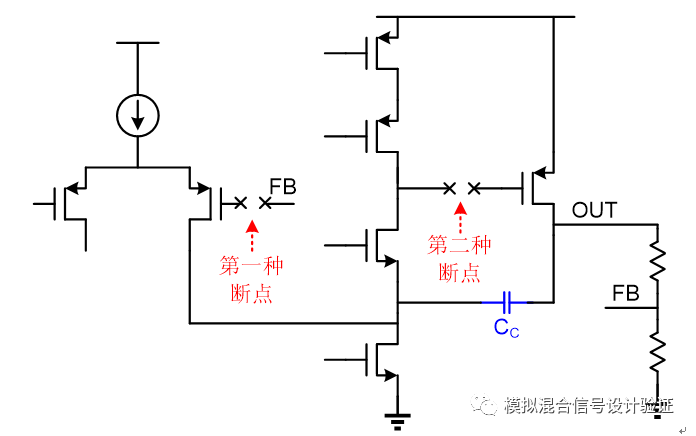
Figure 5
For this example, breaking the loop in the first way is correct, and breaking the loop in the latter way is wrong. So how is the loop actually disconnected? In theory, regardless of whether a path is ascribed to the forward path or the feedback path after the internal disconnection of the system, although the calculated loop curve will be different, the final closed-loop curve calculated should be able to reach the same goal. However, in practice, because many circuits have both feedback and feedforward, but also consider the load and drive effects around the breakpoint, it is easy to cause the simulator to "confuse", so we should try to ensure the integrity of the internal "nested" loop. Sex, breakpoints should also be set in a path that is close to a purely numerical value, such as resistance feedback to the input path, so that the loop gain can be analyzed and compared clearly and simply, avoiding the simulator to iterate a "looks wrong" result. This feature is well illustrated in Fig. 5 of the paper “A Transient-Enhanced Low-Quiescent Current Low-Dropout Regulator With Buffer Impedance Attenuation†(although there is a slight problem with Fig. 5 in the paper, repainting is shown in Fig. 6 below) .
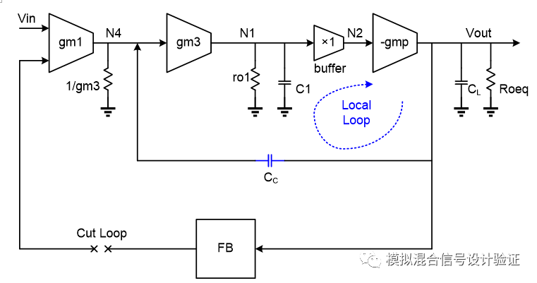
Figure 6
So, for the loop with Miller compensation, I think the most important principle is to keep the integrity of the Miller feedback loop, and set the breakpoint in the path of the constant coefficient as possible to avoid setting the breakpoint. The simulator will be biased in the report in the future! For this example, the reason why the two breakpoint schemes mentioned above are also not possible is that the small loop with Miller feedback is disconnected in this way (the gate input of the second operational amplifier across the capacitor is Disconnected).
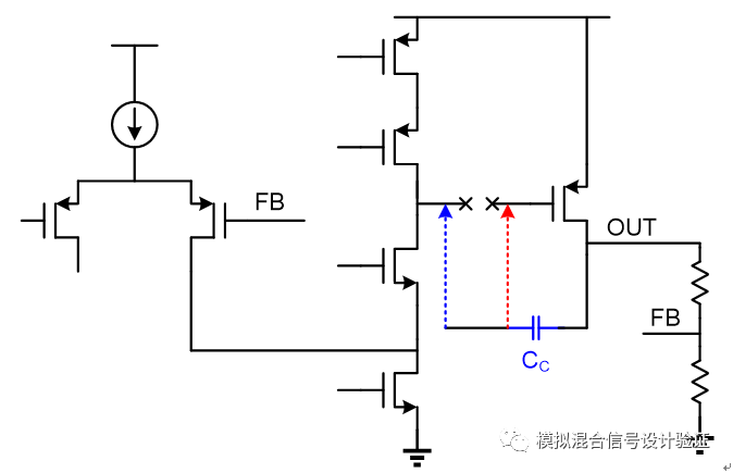
Figure 7
Assuming that the loop breakpoint is also set at the output of the first stage op amp, as shown in Figure 7, only the feedback ends of the Miller capacitors are connected to the left and right sides of the breakpoint, respectively, to obtain completely different simulation results. This is because the integrity of Miller's small loop is maintained when it is connected to the right of the breakpoint. The above mentioned Miller compensation simulation of two different connections has resulted in two huge differences, but also because the loop breakpoint was incorrectly set at the LDO output (trying to set the breakpoint at the output of the first stage op amp The same is true for the end, unless Miller feeds back the point to the right of the loop break to keep the small loop intact. Because the breakpoint destroys the small loop where the Miller compensation is located, the main poles obtained by the simulation of Miller compensation circuits of two different connections become the output poles, and the position of the secondary pole in the circuit is at the capacitive feedback end, and Ahuja connects it. The capacitance-capacitor feedback termination is a low-resistance point and is therefore far greater than the secondary pole seen by the other connection. The reason why the integrity of the Local Loop is ensured is that the input and output impedances have changed due to the feedback. The small loop is integrated into the forward path as a whole. If you disconnect it, you will not be able to obtain this. The characteristics, thus affecting the calculation result of the entire path, will give you a clearer understanding after looking at the analysis of the full article.
The second and third conclusions presented above can actually be attributed to the same problem, that is, the relationship between the Miller pole and the output pole. In simple terms, it is not considered that Miller compensation fails when the Miller pole is close to the output pole. Alright? We all know that using Miller compensation not only produces a Miller pole, but also separates the primary and secondary poles. The Miller effect makes it possible to see an AM-amplifying equivalent capacitor (AM is the open-loop gain of the op amp across the capacitor) at the input of the op amp across which the capacitor is connected, but only for such an understanding It is too simple and crude. On the other hand, when the output load capacitance increases, the amplifier gain across the Miller capacitor will become smaller at the same frequency, causing the gain to fall to 1 at the lower frequency point. As to how much the output load capacitance is, or how much the above gain decreases, Miller compensation will be invalid. Many courses and books do not give a good judgment standard. Often, the output capacitance is very large. . As for the separation mechanism of the two poles, both Razavi and Sansen's books only throw out formulas, and they do not give a simple way to analyze this problem from the perspective of circuit theory. In short, in the course of encountering problems, neither a clear understanding of the thorough Miller effect nor a clear understanding of Miller's compensation mechanism has resulted in many confusions and incomprehensions.
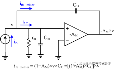
Figure 8
As shown in Figure 8, the classic explanation of the Miller effect and its capacitive equivalent principle is that when the input has a voltage change, a -AM times voltage change is generated at the output due to the effect of the amplifier. It is - (1 + AM) times the pressure difference change, so that this capacitor "looks" larger (1 + AM) times, it is equivalent to an equivalent input (1 + AM) times the input capacitance. We often only pay attention to this equivalent capacitor, but ignore the current flowing through the Miller capacitor is the key to the problem! It is easy to see from Figure 8 that the Miller effect is essentially a voltage detection-current feedback of Shunt-Shunt. I think the best way to understand the Miller effect should be to return to the essence of feedback, and to observe the characteristics of each node's current, you can Get richer content. Comparing a pure capacitor with a capacitor with Miller effect, the equivalent Miller capacitor is AM times because the Miller capacitor "eats" the current at a given input change. AM times, and this multiplication factor AM is totally determined by the open loop gain of the amplifier across the Miller capacitor.
Figure 9
Then, let's look at how the pole is defined. As shown in Figure 9, if we look at the current point of view, the nature of the pole frequency actually means that in a certain node, we let the current flowing through the capacitor be the modulus and flow. The frequency at which the resistor's current modulus is equal. In other words, as the frequency increases, the conduction current flowing through the capacitor increases. When the frequency increases to a certain value, the capacitive characteristic current flowing through the capacitor (the voltage and current have a specific phase difference) is equal to the resistance flowing through the resistor. Resistive current (voltage and current in phase), then this frequency is the so-called pole frequency. From the current point of view, understand the Miller pole concept that is why the Miller effect can make the pole frequency AM times lower. At the same input signal variation amplitude and observation frequency, the current flowing through the Miller capacitor will be AM times that of a pure capacitor. Therefore, to reach the same current as the resistor, the required frequency of the Miller capacitor will naturally be more than a pure one. Small capacitance AM times. The advantage of understanding the Miller pole in this way is that it can be intuitively compared the pole positions and advantages and disadvantages of the Miller compensations of different connections, such as comparing the Ahuja connection and capacitance feedback to the traditional output of the first-level op amp. law. Since the pole frequency depends on the relationship between the signal current, the resistor current and the capacitor current, assuming that the modulus of the signal current is fixed, no matter what the Miller compensation is, at a given frequency, The feedback current flowing through the capacitor remains the same in either connection or the error current flowing through the resistor remains the same, so the pole frequencies of both are equal. The Ahuja connection method generates an error current at the source of the cascode tube at the fold point of the first operational amplifier. This error current flows through the cascode tube and reaches the output of the first-stage op amp. The current gain is “almost†1 during this process. Since the transimpedance gain from the first stage output to the other plate of the Miller capacitor (ie, the output of the op amp to which it is connected) is the same in both cases, the current flowing through the Miller capacitor and the capacitive feedback are generated. The error current ratio is also "almost" the same. As shown in Fig. 10, because of the feedback action, the error current and the feedback current are equalized under two different Miller compensation methods. The error current is the current flowing through the node's resistor, and the pole frequency of both is illustrated. it's the same.
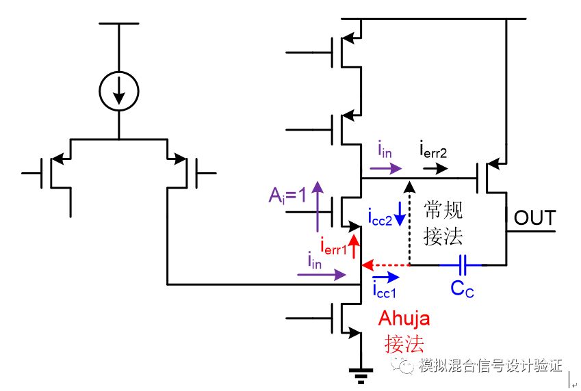
Figure 10
We can further make a corollary: the Miller pole frequency obtained by these different connections is the same, as long as the feedback terminal of the Miller capacitor is connected to the equal current gain in the path while keeping the back transimpedance constant. It's just that the Miller poles are not in the same position on the circuit (but they are all on the capacitive feedback side). For example, inserting more cascode tubes between the folding point of the first stage op amp and the output of the first stage, as shown in FIG. 11 , regardless of whether the feedback terminal of the Miller capacitor is connected to any cascode tube inserted between these two points. For the source, the resulting Miller pole frequency is the same (although the output resistance of the first stage op amp will increase so that the Miller pole frequency is lower than before insertion into the cascode tube, but the comparison capacitor feedback end is in a different connection. The next is consistent). Of course, you can understand the equivalence between the Ahuja connection and the traditional connection from another perspective. For example, in Figure 10, although the open loop gain of the op amp seen by the Ahuja connection capacitor is greater, gm_cas × Ro1 times, but see the output resistance at the source of the cascode tube compared to the output resistance seen at the output of the first stage op amp to be less than ro1/(1/gm_cas)=gm_cas×ro1 times, so the two are offset so that the pole frequency Consistent (gm_cas represents the transconductance of the cascode tube, and ro1 represents the output resistance seen at the output of the first stage op amp). This understanding is actually less clear and accurate, because reaching the pole frequency always depends on the relative relationship rather than the absolute amount, the implied condition is that the two connections make the capacitor current equal to the resistor current at the same frequency, the same input At the signal current, the voltage they generate at the current summation node differs depending on the output impedance.
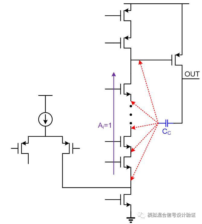
Figure 11
Once you understand the principle of the Miller effect from the perspective of current and feedback, you will find everything will suddenly become clear. Obviously, in the section of the path that Miller capacitor feedback may be connected to, finding the front end of the equal current gain on the path is a more effective Miller feedback connection, because the two poles are connected across the capacitor while keeping the Miller pole constant. The terminal voltage gain AM may not be the same. For example, we can see from Figure 10, compared to the traditional connection, Ahuja connection AM to be gm_cas × ro1 times, this will bring two advantages: one due to the relationship between feedback and low resistance point to start the establishment of the process It's easier; the second is the effect on the output pole, which is another issue we want to discuss next.
Let's look at how to understand the separation of the poles. Many papers and books will directly throw a formula to tell you that the derivation is such a conclusion. For example, in Sansen's book, we first give formulas and approximate conditions, and then give a The result of the calculation leads to a conclusion: "If a change in a parameter in the circuit causes a change in coefficient a, both poles will be affected and move in the opposite direction, which is the theoretical basis of the pole separation", although the book A graph was also given to depict the entire separated trajectory process, but I believe that when you see the above text image, there will still be a mmp in mind, because it does not explain which parameter "a certain parameter" is, nor does it have. Explain the slope, pitch, and inflection of the line in the graph. On the other hand, although we know that Miller compensation may fail when the output capacitance is large, how large is this “largeâ€, and is there any judgment condition? From the feedback point of view, this problem becomes easier to understand: When the frequency is greater than the Miller pole frequency, Miller capacitance feedback coefficient is close to 1 (assuming Miller compensation small loop op amp input node parasitic capacitance is small), at this time the whole The feedback loop is fully established. The loop gain T=AM×fM. As long as T is sufficiently large at this frequency, the output equivalent resistance RLeq will be reduced by (1+T) times due to the feedback of this small loop. About 1/gmp (gmp is the output-level transconductor), then the output pole is pushed away by (1+T) times. This conclusion has been calculated specifically in the ninth chapter of Gray's book. Because the Miller effect causes the main pole to be lower AM times, and the output pole is pushed by about AM times due to the Miller effect, an AM separation of about 2 times is obtained overall. Miller compensation will then fail depending on whether the small loop gain seen at Miller's pole frequency is much greater than 1, as shown in Figure 12. Gain-bandwidth product can be used to simply evaluate how much AM can make enough separation Far (assuming that the miller pole before separation is m times higher than the output pole), that is, the output pole should be at least ATOT multiple of the Miller pole (the total gain of the entire op amp), ie, AM2/m>ATOT=gm1/ CC, gm1 represents the transconductance of the input pair of the first op amp, and CC represents the Miller capacitance. For example, when the Miller capacitance feedback termination is connected to the high-impedance output point of the first stage operational amplifier (the output resistance is ro1), AM=gmpRL, m=(RLCL)/(ro1CC), so CC>1/gmp×√ ((gm1) ×CL)/(ro1 ×RL)) where RL and CL represent the equivalent resistance and load capacitance of the entire LDO output stage, respectively. Under our application conditions, the CL is very large, and the parasitic capacitance of the CC is larger than that of the feedback node it is connected to. Therefore, some analysis has been simplified to obtain some simple results. Special instructions will default to such capacitor conditions. When the magnitudes of these capacitances in the circuit are relatively close to each other, these special results can be replaced by "degenerate" the equivalent capacitance under the actual circuit.

Figure 12
Seeing here, somebody will certainly have such a question: The output resistance is reduced by (1 + T) times because of the feedback, then input resistance is also the same will be reduced (1 + T) times? As a result, isn't the reduction in the input resistance "muting" with the multiplier of the Miller capacitance? Gray did not give an explanation. Perhaps he thinks the problem is too simple. In short, we know that this is obviously not the case in practice, so we tried to do the following analysis.

Figure 13
From the low frequency to the high frequency, we carefully look at the whole process of Miller compensation change. First, at low frequencies, the feedback coefficient of the Miller capacitor is very small, and the loop gain T is very small, so most of the signal current acts as an error current. The input resistor that flows into the op amp produces a large voltage drop across the capacitor, but because of the low frequency, the current through the Miller capacitor is much smaller than the current through the input resistor. As the frequency increases, a frequency point can always be found so that the current flowing through the Miller capacitance is equal to the current flowing through the input resistor. Although the feedback coefficient is very small at this time, the loop gain T is 1 and thus the input resistance is hardly reduced. This is in line with the original expectation. A simplified approximate calculation is performed as shown in Fig. 13 without considering the load effect. Loop gain T is one. As the frequency continues to increase, the current flowing through the input resistor is getting smaller and smaller, and the input impedance gradually dominates by the parasitic capacitance at the input. Therefore, the feedback coefficient is very close to 1 due to the voltage divider of the capacitor (considering that the Miller capacitance is much larger than In the case of parasitic capacitance of the node), the loop gain T is already large enough so that the input and output impedances are reduced by (1+T) times. However, when the input impedance is reduced by a capacitive part, that is, the capacitance is increased by (1+T) times, the input impedance seen by a current feedback system will become smaller because of the input of the same size. Under the current signal, most of the current is shunted by the feedback network and the current into the op amp is very small, resulting in a very small input voltage. The current that is "eaten" by the feedback network is the capacitance that flows into the input terminal and belongs to the capacitive component. Therefore, this does not change the position of the Miller pole, but it pushes away the output pole! The equivalent impedance of the output pole is also reduced by feedback. Why does it reduce the resistive impedance instead of the capacitive impedance? First of all, we know from the output point of view, no matter whether the Miller capacitor CC or the load capacitor CL has a “multiplication†effect due to feedback, that is, when there is a change in the output voltage, there is no effect of this feedback. The current flowing through them is the same. So what is the so-called "reduced output impedance due to feedback?" This is due to the fact that under the same current input signal, due to feedback, when the loop gain is large enough, most of the input current flows through the feedback network to the output, causing the “error current†input to the op amp to change. It is (1+T) times smaller, which results in the output voltage signal being smaller (1+T) times than when there is no feedback. Equivalently speaking, under the same output voltage change, the output resistance + feedback network "eat" current is (1+T) times larger than when there is no feedback. Although the feedback network shunt's current is a capacitive current, but because the entire feedback system first encounters the Miller pole, when we increase the “observed frequency†above the Miller pole frequency to find the next pole, we see at the output stage. The signal current itself should be a capacitive current, which means that the capacitive current flowing from the input shunt to the feedback network where the Miller capacitor is located is consistent with the signal current. We can understand from another point of view that when the frequency is higher than the Miller pole, the current flowing into the capacitive part of the input terminal will be more and more current than the current flowing into the resistive part, so that the input voltage signal flowing into the system will follow The phase relationship of currents more and more shows the "phase relationship of the capacitive nature". If such a phase relationship is exhibited at the output of the system, it shows that the overall composition of the amplifier and the feedback network shows a resistive characteristic (holding The input and output voltage and current phases do not change. That is, the feedback makes the entire equivalent resistive part of the impedance seen at the output smaller, thus pushing the output pole farther.
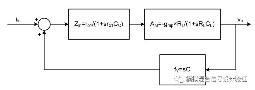
Figure 14
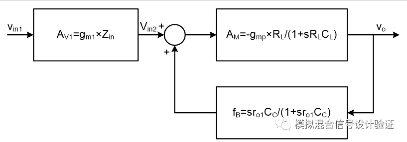
Figure 13 is just a very simplified approximation of the calculations used to illustrate Miller pole and output pole with compensation changes, the following detailed analysis from the perspective of the system topology, such as Figure 13 such a system structure with Miller capacitance compensation can be used Topology is represented in 14. Wherein ro1 represents the input resistance Rin in the figure can be regarded as the input resistance of the op amp, assuming Cpara is negligible compared to CC, so the system looks into the open-loop input impedance Zin after taking into account the influence of the feedback network load is the input resistance Parallel connection of capacitors CC. If we only want to see the effect of the forward AV and feedback networks on the separation of the poles from the perspective of the input voltage to the output voltage, then we can do a simple transformation to get the topology of Figure 15.

Figure 15
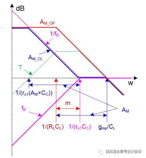
Figure 16
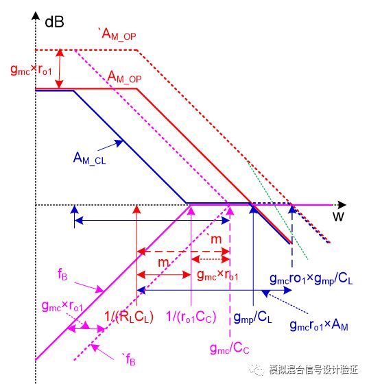
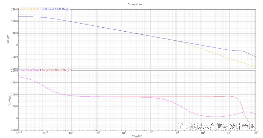
As the saying goes, a thousand words are not as good as a picture. We can use the open loop voltage gain AM, feedback network voltage gain fB, its inverse 1/fB, and loop gain T=AM×fB for each part in Figure 15. The closed-loop gain parameters of the entire system in the red box are plotted as a function of frequency, and they are combined together. An approximate transfer function curve of the Miller compensation small loop can be obtained as shown in Figure 16. The red AM_OP in the figure represents the open-loop gain curve of the op amp across both ends of the Miller capacitor. AM represents its DC value; purple fB represents the gain curve of the feedback network; and green T represents the loop gain of the system included in the red box in Figure 15. The curve; the blue AM_CL represents the closed-loop gain curve of the system contained in the red box in FIG. The lines in Fig. 16 are more complicated, but if you can understand the meaning of all lines, inflection points, and slopes, then the Miller effect and Miller compensation can be understood. It is easy to see from the figure that the loop gain T exceeds 1 at the Miller pole and falls back to 1 at the output pole that is pushed farther away. The entire closed-loop system follows the curve 1/fB in the middle part where T is much greater than 1. When the two heads T are much smaller than 1, the curve AM_OP is followed. Therefore, the blue closed-loop gain curve has two poles, namely the compensated Miller main pole and the output output subpole at unity gain. The whole curve shows a “quasi†integrator. In the form of low-frequency op amp gain, the gain after the main pole monotonically decreases until unity gain, and the gain after the secondary point continues to decrease (since only the characteristics of the system in the red box in FIG. 15 are not taken into consideration for the input impedance Zin. There is a platform with a gain of 1 compared to the true integrator curve). From the figure we can clearly see the separation of the two poles, and it can also be confirmed that when the loop is disconnected for simulation, the integrity of the compensated small loop with Miller capacitors should be maintained, that is, because the feedback The reason for its closed-loop nature needs to be viewed as a whole. The distance after the two poles are finally separated is AM2/m. Imagine moving the pink feedback network gain curve left and right. It is not difficult to find that the condition that Miller compensation is still implied is m>AM, that is, ro1CC. Figure 17 Figure 18 Figure 19 Starting from Figure 16, we can further analyze and compare the Miller compensation of the Ahuja connection with the Miller compensation of the conventional connection, as shown in Figure 19. Compared to conventional connections, the Ahuja connection moves the output of the first stage op amp to the source of the folded cascode transistor of the first-stage op amp. Therefore, the gain of the op amp across the capacitor is larger than that of the gmc. ×ro1 times. Where gmc represents the cascode transconductance, and ro1 represents the output resistance of the first stage op amp (parallel to the output impedance of the upper and lower cascode structures). Since the current gain between the two nodes is 1, the cascode source can be known. The output resistance of the terminal should be smaller by gmc×ro1 times. From the figure, we can see that the zero point of the feedback network has moved to the right by gmc×ro1 times, from the pink solid line to the pink dotted line, and the same reason can push the changes of other curves, and finally we can see The position to the Miller pole has not changed and the output secondary point has been pushed further. At this point, we can clearly understand the advantages of the Ahuja connection, because the open loop gain AM of the amplifier loop where Miller compensation is located is gmc×ro1 times larger than the conventional connection, although the m value in the figure is also so much larger. Times, but the distance after separation is AM2/m, and the overall size is increased by gmc×ro1. This is because the output pole is pushed farther than it is! Similarly, we can include the previous input impedance Zin and the previous transconductance gm1 to draw a curve similar to the one on the right side of Figure 18, except that the secondary points will be pushed farther. The specific simulation results are shown in Figure 20. Here, a question arises: Is it possible to push the compensated unity gain bandwidth even further by simply inserting more cascode pipes in the middle of the circuit across the Miller capacitor? This obviously is not feasible because the cascaded cascode structure will generate a large output impedance at the drain of its last MOS tube and introduce it into the AM so that it no longer maintains a single-pole curve before the unity-gain bandwidth. As shown by the green line in Figure 19, it is possible to influence the distance, bandwidth, and stability of the secondary point being pushed farther. In order for AM not to introduce too many secondary points, inserting multiple single-stage op amps in the middle may be a better choice, so I guess Nested Miller compensation is probably based on this consideration, similar to a multi-stage cascading Buffer circuit. The intention is to rationally allocate the driving ability between different levels. Some of the thoughts on the Miller effect and compensation in this paper are believed to be helpful for understanding the Nested Miller compensation, but the specific principle should still need to find answers from Huijsing's book. Figure 20 Through the above in-depth analysis, we can find a better understanding of the Miller effect and Miller compensation from the current and feedback point of view, and also obtained some intuitive understanding and conclusions: 1. Simulation analysis should be kept in the open loop Miller compensates for the integrity of the small loop, because the nested internal closed loop will affect its input and output impedances, while setting the breakpoint as much as possible in the position of the pure coefficient feedback; 2. Miller equivalent input capacitance is caused by the span It is determined by the open loop gain of the op amp at both ends. 3. As long as the subsequent transresistance is consistent, the feedback terminal of the Miller capacitor is connected to any equal current gain position in the path before the transimpedance. The Miller pole frequency; 4. The output pole Because the Miller feedback function is pushed far (1+T) times, you can use Figure 12 or Figure 16 from the perspective of the gain-bandwidth product to calculate how much effective Miller capacitance the pole separation requires and Compensate for the loop gain T in the small loop. It is not certain that the loop gain can be compensated. Under any conditions, it will be invalid. 5. The advantages of Ahuja connection method are many, and there is no clear indication Significant disadvantages; 6. By shifting a DC voltage (such as with a source follower) and with the amplification or reduction of the feedback factor, both ends of the Miller capacitor can be placed in the appropriate voltage domain, through the impedance transformation (for example, insert A source follower can isolate the feedforward effect of Miller capacitance, or introduce feedback only or introduce feedforward only. 7. Try to use these thoughts about individual Miller feedback to further help analyze and simplify the principle of Nested Miller compensation, such as integrating the innermost Miller loop as an integral integrator, as in Figure 16 and Figure 18. Step-by-step "combination" of the gain curve of the final entire forward path. At this point, although it can not be said that Miller compensation has been fully understood, it can effectively help us to see some of them through some meaningful thinking, and provide some useful criteria and simplify calculations in specific practices. result. Although the whole process was a little brain-burning, it took a few nights to finally write these words. Finally, I would also like to thank my colleagues Jiang Wenping, Maggie and Jin Jin for their enthusiastic help, discussion and advice! TO-220 Transistor Outline Package is a type of in-line package often used in high-power transistors and small and medium-sized integrated circuits.
It not only plays the role of mounting, fixing, sealing, protecting the chip and enhancing the electrothermal performance, but also connects to the pins of the package shell with wires through the contacts on the chip, and these pins pass through the wires on the printed circuit board. Connect with other devices to realize the connection between the internal chip and the external circuit.Because the chip must be isolated from the outside world to prevent impurities in the air from corroding the chip circuit and causing electrical performance degradation. On the other hand, the packaged chip is also easier to install and transport.
TO-220 package is a kind of in-line package that is often used for fast recovery diodes. TO-220AC represents a single tube with only two pins and only one chip inside.
The diodes are packaged in TO-220AC and can be used in switch mode power supplies (SMPS), power factor correction (PFC), engine drives, photovoltaic inverters, uninterruptible power supplies, wind engines, train traction systems, electric vehicles and other fields.

TO-220 package,Super Fast Recovery Rectifiers,Fast Rectifiers Diode,Ultra Fast Rectifiers
Changzhou Changyuan Electronic Co., Ltd. , https://www.cydiode.com