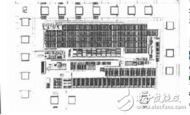
The distinction between IC front-end design (logical design) and back-end design (physical design):
Front-end design focuses on the logical structure of the chip, while back-end design deals with the physical implementation. From a design perspective, the output of front-end design is a gate-level netlist that represents the circuit at a logical level.
Front-end design process and EDA tools used 
1. Architecture Design and Verification
This step involves defining the overall system architecture based on the requirements. Simulation of the architectural model can be done using Synopsys’ CoCentric, which is a System C-based simulation tool.
2. HDL Design Input
Design input can be done through HDL languages like Verilog or VHDL, circuit diagrams, or state transition diagrams. Tools such as Active-HDL are commonly used for this purpose, while LEDA from Synopsys helps in RTL analysis.
3. Pre-simulation (Functional Simulation)
This step ensures that the design meets the functional specifications before moving to synthesis. Tools like VCS (Synopsys), ModelSim (Mentor), Verilog-XL (Cadence), and NC-Verilog (Cadence) are widely used for this purpose.
4. Logic Synthesis
Logic synthesis converts the HDL code into a gate-level netlist. This process requires setting constraints related to timing, area, and other performance metrics. The choice of library also affects the final timing and area. Before synthesis, a pre-simulation is performed, followed by post-simulation after the synthesis is complete. Popular tools include Synopsys’ Design Compiler, Cadence’s PKS, and Synplicity’s Synplify.
5. Static Timing Analysis (STA)
STA checks whether the circuit meets setup and hold time requirements. PrimeTime from Synopsys is a widely used tool for this task.
6. Formal Verification
Formal verification ensures that the synthesized netlist matches the original HDL design functionally. One common method is equivalence checking, where the functionality of the HDL design is compared with that of the netlist. Synopsys’ Formality is a popular tool for this purpose.
Back-end design process and EDA tools used:
1. Data Preparation
For tools like Silicon Ensemble, the back-end design requires standard cell libraries, macro cells, and I/O pad files provided by the foundry. These are typically in the form of LEF, TLF, and V files. After front-end synthesis, a gate-level netlist, timing constraints, and a DEF file are generated. For Synopsys’ Astro, the STP file serves as the gate-level netlist. Other files include TDF, TF, and FRAM, CELL, LM views for standard cells and I/O pads.
2. Floorplan
This step involves placing standard cells, I/O pads, and macro cells. I/O pads are placed first, while macros are positioned based on timing requirements. Standard cells are placed automatically within a defined area. Once floorplanning is complete, the chip size, core area, row layout, power ring, and strip are determined. PNA (Power Network Analysis) can be used to check IR drop and EM issues during placement.
3. Placement
After floorplanning, the positions of macros, I/O pads, and standard cells are fixed. The SE passes data to the Physical Compiler via a DEF file, which uses the DB file to get the netlist and timing information for automatic placement. Timing checks and optimization are also performed during this phase.
4. Clock Tree Synthesis (CTS)
The clock tree drives all the flip-flops and registers in the design. To reduce skew and balance delays, buffers are inserted along the clock network. This process is often repeated to achieve an optimal clock tree.
5. STA and Post-simulation
After clock tree insertion, parasitic parameters are extracted and passed to PrimeTime for static timing analysis. If no violations are found, the results are sent back to the front-end team for post-simulation. In Astro, starRC XT is used for parameter extraction after detailed routing.
6. ECO (Engineering Change Order)
ECO allows for small changes to fix timing or functional issues identified during STA or post-simulation.
7. Filler Insertion
Fillers are used to fill gaps between standard cells and I/O pads. They help meet DRC rules and ensure proper diffusion layer connections.
8. Routing
Routing involves connecting all the components under process rules, including wire width, spacing, and insulation. It is performed with timing-driven conditions to minimize wire length on critical paths.
9. Dummy Metal Addition
Foundries require a minimum metal density to prevent over-etching. Dummy metals are added to maintain this density and improve performance.
10. DRC and LVS
DRC checks the layout against design rules, including spacing and width, while LVS verifies that the layout matches the netlist. Tools like Synopsys’ Hercules, Mentor Calibre, and CDN Dracula are commonly used for these checks.
11. Tape Out
The final GDSII file is sent to the foundry for mask fabrication after all checks and verifications are completed.

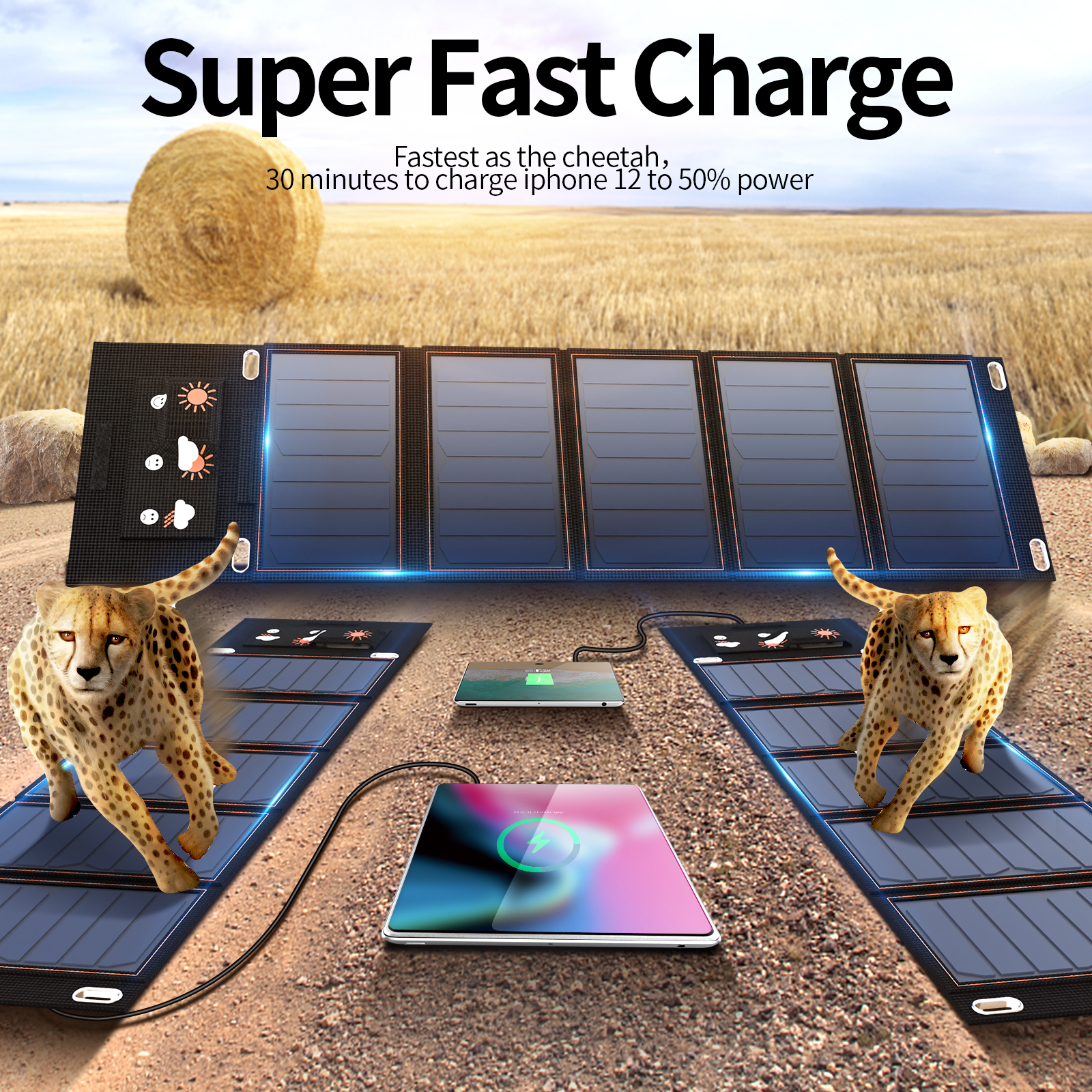
A solar cell panel, solar electric panel, photo-voltaic (PV) module, PV panel or solar panel is an assembly of photovoltaic solar cells mounted in a (usually rectangular) frame, and a neatly organised collection of PV panels is called a photovoltaic system or solar array. Solar panels capture sunlight as a source of radiant energy, which is converted into electric energy in the form of direct current (DC) electricity. Arrays of a photovoltaic system can be used to generate solar electricity that supplies electrical equipment directly, or feeds power back into an alternate current (AC) grid via an inverter system.
Solar Panel,200w Folding Solar Panel,Folding Solar Portable Power Station,Sunpower Solar Cell
suzhou whaylan new energy technology co., ltd , https://www.xinlingvideo.com