The difference between front-end design (logical design) and back-end design (physical design) in IC development lies in whether the design is process-dependent. From a design perspective, the outcome of front-end design is a gate-level netlist that represents the logical structure of the chip.
Front-end design involves several key stages, each utilizing specific EDA tools. The first step is **architectural design and verification**, where the system is broken down into modules. This phase often uses Synopsys' CoCentric, a System C-based simulation tool. Next comes **HDL design input**, which includes writing code in Verilog or VHDL, drawing circuit diagrams, or using state transition diagrams. Tools like Active-HDL and Synopsys' LEDA are commonly used for this stage.
Following this is **pre-simulation** (also known as functional simulation), where the design is tested against its specifications before synthesis. Tools such as VCS, ModelSim, Verilog-XL, and NC-Verilog are used to validate the functionality. Then comes **logic synthesis**, where the HDL code is converted into a gate-level netlist. Constraints such as timing and area are applied during this process, and the choice of library significantly affects the final performance. After synthesis, **static timing analysis (STA)** checks for setup and hold time violations using tools like PrimeTime from Synopsys.
Another critical step is **formal verification**, where the synthesized netlist is compared with the original HDL design to ensure functional equivalence. Synopsys' Formality is a popular tool for this purpose.
On the back-end side, the design moves toward physical implementation. The **data preparation** phase involves gathering standard cell libraries, macro cells, and I/O pad files from the foundry, typically in formats like LEF, TLF, and V. The front-end netlist, along with timing constraints, is used to generate a DEF file for back-end planning.
**Layout planning** determines the placement of standard cells, I/O pads, and macros based on timing and area requirements. Tools like Silicon Ensemble and Physical Compiler help automate this process. **Clock Tree Synthesis (CTS)** ensures balanced clock distribution by inserting buffers to minimize skew.
After placing all components, **static timing analysis** and **post-simulation** are performed to verify timing accuracy. If issues are found, an **ECO (Engineering Change Order)** may be implemented to fix them. **Filler insertion** helps meet DRC rules by filling empty spaces between cells and I/O pads.
**Routing** connects all components while adhering to manufacturing rules, ensuring minimal wire length on critical paths. **Dummy metal** is added to maintain uniform metal density and prevent etching issues. Finally, **DRC (Design Rule Check)** and **LVS (Layout vs. Schematic)** ensure the layout complies with design rules and matches the original netlist. Once everything is verified, the final **GDSII file** is sent to the foundry for fabrication.
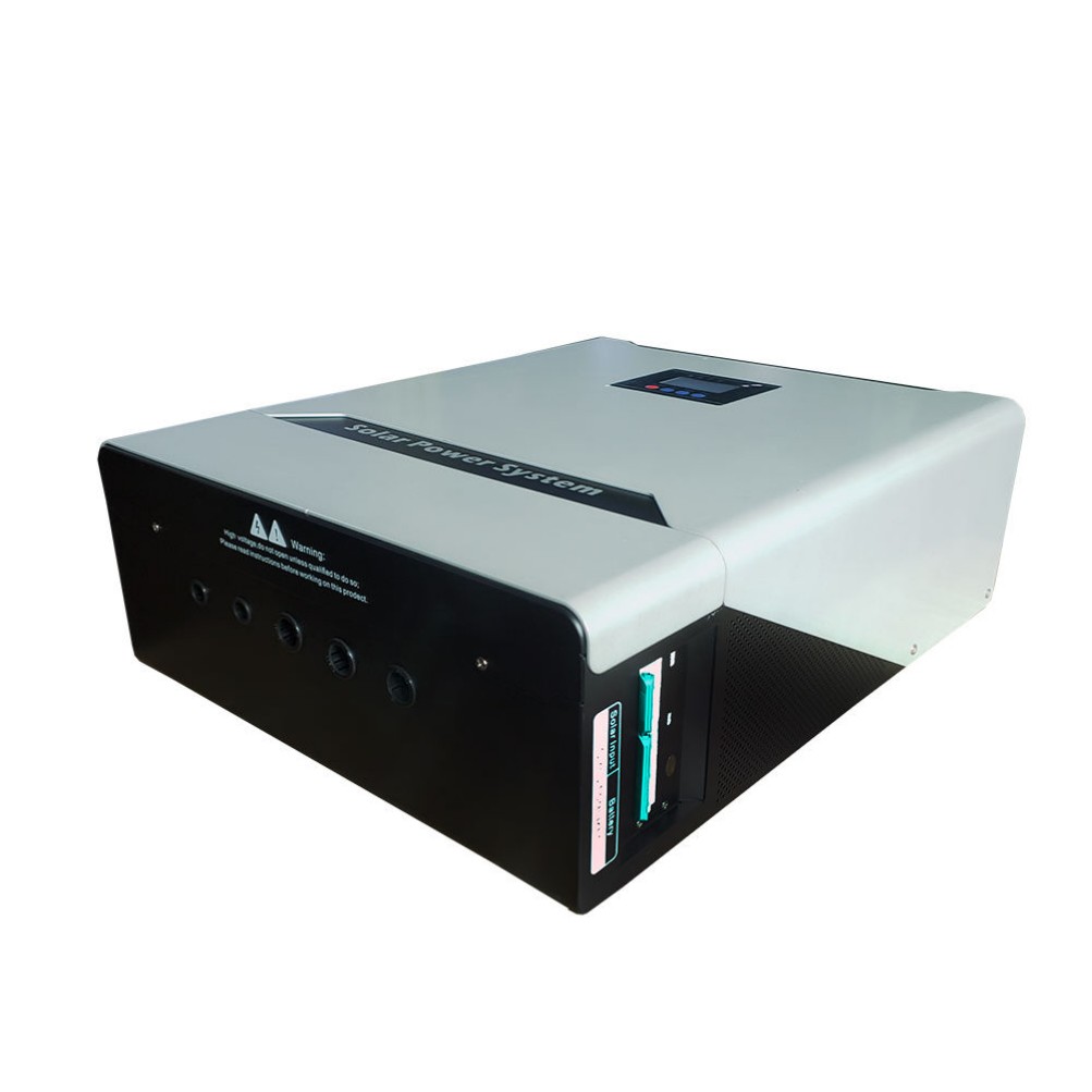
1KW-6KW Hybrid Inverter(with MPPT Charge)


1KW-6KW MPPT Hybrid Inverter,Solar Inverter With Mppt Charge,Hybrid Mppt Charge Solar Inverter
suzhou whaylan new energy technology co., ltd , https://www.xinlingvideo.com