At present, almost all household electricity, industrial and commercial electricity, or public electricity use almost all AC power. When a conventional DC-LED is used for lighting, AC-DC converters must be provided to convert AC power to DC power. The advantage of this power supply mode is that the direct current stability is good and the LED can emit light continuously.
However, in the actual application process, the use of AC-DC conversion devices has also brought many other problems, such as: 1, AC-DC conversion process, there are 15 to 30% of the power consumption, resulting in unnecessary power waste, Compared with the characteristics of LED high efficiency and energy saving; 2, AC-DC conversion device cost is higher, virtually increase the user's cost; 3, AC-DC conversion device in the short life of Electronic Components can not be up to ten with the LED The life span of a few years is matched; 4, LED is in uninterrupted working condition while driving in direct current, will produce a large amount of thermal energy, thus cause the device to produce the serious light decay.
In view of the deficiencies of the above traditional power supply methods, many companies hope to solve the above problems by using AC-LEDs. AC-LED uses the principle of rectifier circuit, so that the LED can work directly under AC power. However, since the alternating current is periodically changed, the LED emits a strobe when it emits light.
There are two main existing solutions. First, the series circuit is used to improve the waveform, which can effectively improve the power factor, but it also reduces the efficiency. Secondly, the use of parallel circuit filter capacitors can reduce the strobe, but at the same time it brings about a limitation of life. And reduce the power factor.
Recently, Sichuan Xinli Light Source Co., Ltd. (hereinafter referred to as Xinli Light Source) has used newly developed phosphors. When the current cycle changes, the delay of the phosphor brightness can be used to compensate for the strobe light emission and effectively solve the problem of AC-LEDs. technical challenge.
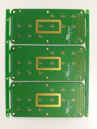
6-layer Blind & Buried PCB Board , Base Material: FR4 S1000-2(TG 170). Inner copper thickness 1 oz and outer 1.5 oz finished. the surface treatment is Immersion Gold 2U" with matt green colour solder mask. White colour Legend.board thickness 1.2 mm. Min.line width/Min.line spacing 0.1/0.1 mm. E-test: 100%. With L1-L2 & L5-L6 blind vias. and L3-L4 buried holes. It is a typical Mechanical Blind & Buried PCB board.
We can make laser and mechanical Blind & Buried PCB Board(no cross-shaped) with the material FR4 or FR4+Rogers mixed material Circuit Board.

Blind & Buried PCB Board,Customized Buried PCB Board ,Copper Double Sided Board,Blind Buried Via PCB
Orilind Limited Company , https://www.orilind.com