The advanced processes used by IMFT can dramatically change the way consumer electronics are designed and used. These high-density, high-performance flash devices enable Intel-backed Robson flash caching technology and hybrid SSD/HD systems (supported by Microsoft, Sandisk, and Seagate). These technologies are likely to appear in products that require large amounts of memory, such as desktops and laptops. Micro MLC NAND flash devices can store large amounts of data, and these devices can hold data without power. Because there are no moving parts in the flash memory device, it is more resistant to vibration than the hard disk and may eventually replace the hard disk. This ruggedness is ideal for mobile applications, especially automotive applications such as GPS navigation systems and high-end automotive entertainment systems.
This article refers to the address: http://
Flash memory with hybrid HD or Robson flash caches can access data 100 times faster than traditional USB flash drives, which helps improve the mobility and functionality of mobile devices such as cell phones and PDAs. Other products, including USB flash drives, MP3 players, digital cameras, navigation systems, and data recorders, will also benefit from these next-generation flash devices.
If you are loading from flash instead of hard disk, typical Microsoft Word documents will be opened in less than a tenth of a second (even for very large documents, no more than 5 seconds), and Windows XP does not start at the same time. It will last for more than 15 seconds and has the inherent reliability of replacing all moving parts with one component. The advantages of flash memory are not limited to these. With digital camera memory cards, if you read and write about 1000 photos a day, you can use them for up to 7 years before they need to be replaced. So this card has the opportunity to be reused in new cameras before it really goes to bed.
Departing from 50 nm
To meet the high expectations of the Intel-Mexico cooperation program, IMFT must narrow the technology gap with key competitors Toshiba and Samsung. Semiconductor Insights detailed in its September 2006 report that IMFT has worked hard to release 50nm, 4Gb SLC flash memory products in the third quarter of 2006. It is clear from the analysis report that IMFT abandoned the traditional strategy adopted by its two parent companies. Micron has changed from a cost and manufacturing innovator to an innovative company with cutting-edge technology. This change is enormous.
However, IMFT does not completely bridge the above gap, and it is still a little bit worse. Competitor Toshiba has been using MLC technology to optimize memory density, enabling 8Gb, 70nm flash process technology to achieve memory bit densities of up to 56.5Mb/mm2. IMFT's 4Gb SLC flash devices cannot reach Toshiba's 41.8Mb/mm2 density even with its advanced 50nm technology.
IMFT's 4Gb devices are fabricated in three-layer metal, three-polymer, and 50-nm CMOS processes. Although Micron has long implemented copper connections in the DRAM interconnect process, IMFT uses a more conservative aluminum interconnect process in metal layers 2 and 3, while metal layer 1 uses an innovative tungsten via priority. Dual damascene technology.
A special shallow trench isolation process for 4Gb devices can be used to implement triple gate oxide process technology with alternating polysilicon capacitor structures. This is an innovative isolation method: a gate dielectric is formed before the active area hard mask/STI polishing barrier layer is formed. IMFT uses a polysilicon hard mask (similar to a nitride top layer) to replace traditional silicon nitride, so the difference from the traditional method is more extensive.
After STI etching, filling and leveling, an inlaid polysilicon layer coplanar with the isolation surface is formed. In areas where thick high-voltage oxides are grown, this polysilicon layer is used as a low-profile plate for polysilicon capacitors and has a high-quality CMP finish interface. Shielded removal of the subsequently deposited ONO capacitor dielectric provides the contact area of ​​the second polymer layer to the lower capacitor plate. In the region where the transistor gate electrode will be formed, the ONO layer will be completely removed.
16Gb super big change
IMFT's "next generation" 50nm 16Gb MLC process is actually a less stringent "approx. 40nm" process technology. Like the previous generation technology, this device is also manufactured using a three-layer metal, three-polymer process. Roughly speaking, this claimed 50nm 16Gb MLC device is nothing special, and even feels that it is too late to launch (think about how long it has been since the launch of 4Gb SLC flash products). However, this is only a superficial phenomenon. To really understand how much this product differs from the early 50nm products, it is necessary to understand the inside of the device in detail.
First, IMFT engineers have moved from aluminum-based interconnect technology to copper interconnect technology. This new process will make it easier to adjust the metallization layer to accommodate designs that are close to 40 nanometers. Metal layer 1 formed using tungsten via-first dual damascene technology can be easily transferred from the 4Gb version to the new 16Gb flash device; we can see if metal layer 1 will be used for the second time in the 40nm process.
IMFT also modified the integration sequence for shallow trench isolation. This modification provides scalability for effective area spacing in the memory array (which is critical for IMFT to drive next-generation process nodes), which is well studied by Semiconductor Insights. Interestingly, although this modification allows for scaling, some of the steps in this sequence do not seem to have any technical advantage. One can't help but wonder if this approach is to avoid the STI process sequence that other flash providers have.
Finally, almost 20% reduction in array polymer width on this device should reduce capacitive coupling in the array and improve overall power and speed performance. This will further determine the process for the next generation of technology nodes, especially if low-k materials are used to further reduce coupling in the memory array.
Uncover the appearance
Toshiba and IMFT's 16Gb MLC NAND flash devices have different details behind them. Toshiba achieved an impressive 94.5Mb/mm2 memory bit density on its 16Gb, 56nm MLC devices; however, IMFT achieved a density of 98.7Mb/mm2 on its 16Gb MC devices, surpassing Toshiba's storage. The bit density is almost equivalent to the 101.7MB/mm2 storage density of competitors' 51nm, 16Gb NAND devices.
Coupled with the fact that the width of the floating gate of IMFT has been reduced by 20%, you will not be surprised to see that they will be sampling early next year with a new process that has been slightly modified for the current 50nm process. From a larger perspective, each technology migration allows us to move closer to more cost-effective solid-state drives. When we achieve transcendence, new consumer products will emerge and demand for higher capacity in semiconductor technology. We have benefited a lot from the semiconductor industry in the past few years, and I am very much looking forward to such technological advances.
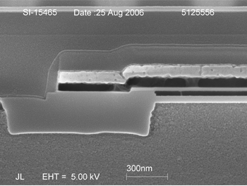
Figure 1: Polysilicon capacitor structure. The black line at the bottom is the low polysilicon plate
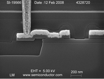
Figure 2: Polysilicon capacitor structure for 16Gbit flash memory, showing the low-level board connector. IMFT's 4G, 16Gbit NAND flash memory
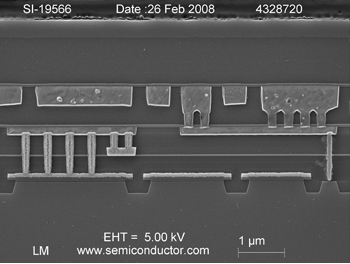
Figure 3: Metal layer 2 and layer 3 of IMFT's 16Gbit MLC flash memory use copper dual damascene process, metal layer 1 uses tungsten dual damascene process
Led Panel Light is a high-end interior lighting, the outer frame made of aluminum alloy by anodic oxidation, the light source is LED, lighting design simple and beautiful, luxurious atmosphere, both good lighting effects, but also brings beautiful feeling. Unique design LED panel 18w light, the light guide plate after a high light transmittance to form a homogeneous plane glow effect, illuminance uniformity is good, light, soft, comfortable yet bright, can relieve eye fatigue. LED indoor panel lights can also radiation, will not stimulate the pregnant women, the elderly, children's skin.


LED Panel light Installation form:
1, can be mounted on the ceiling, walls and installation of surface;
2, LED Panel light may be suspended under the ceiling or mounting body. When mounted on a white ceiling, the entire ceiling was the same color, very beautiful, clean and coordinated;
3, LED panel light using broadband voltage design (AC85-240V / 50-60Hz), can be used in all countries of the world; high-power LED with isolated power, constant current or constant voltage drive, high power efficiency, power clean, stable performance ,Safe and reliable;
4, LED panel light are similar LCD TV backlight technology, a new type of surface light source, light and soft, beautiful appearance, has been widely favored by European and American businessmen, a large number of foreign investors are Buying good quality, good service, good price led Panel Light and suppliers;
Application:

Packing with paper boxes:

Mingxue Optoelectronics Co.,Ltd. has apply the I S O 9 0 0 1: 2 0 0 8 international quality management system certificate, for led panel light we apply the CE, RoHS and SAA certificate for our led lighting product.


Led Panel Light
Led Panel Light,Led Ceiling Panel Light,Square Led Panel Light,Outdoor Led Panel Light
Shenzhen Mingxue Optoelectronics CO.,Ltd , https://www.led-lamp-china.com