As brightness and energy efficiency increase, extending the lifespan has become one of the main factors driving the rapid development of high-brightness light-emitting diode (HB-LED)-based solid-state lighting design. However, not all HB-LEDs are comparable in these respects, and the way manufacturers apply electrostatic discharge (ESD) protection may be a critical factor influencing the lifetime of HB-LEDs. In this article, ON Semiconductor's VidyaPremkumar will discuss the importance of ESD protection and explain the latest advanced protection technologies that HB-LED module manufacturers are using to ensure that their designs will optimize their lifetime and quality potential.
Introduction: Threats beyond the evolution curve
The commercialization of green and blue LEDs, combined with the steady and rapid increase in the average light output of each device achieved in recent years, has opened up a large number of new application markets for solid-state lighting. The price and performance of HB-LEDs have surpassed Haitz's Law, which is similar to Moore's Law for transistor density; according to this law, the LED's light output level doubles every 2 years, averaging the cost per lumen of light output. It will be reduced 10 times every 10 years.
In fact, the light output of LEDs is now doubled every 18 months or even less. Today there are devices with a luminous efficacy of 120 lm/W, and leading laboratories have even demonstrated a luminous efficacy of 200 lm/W. LED.HB-LED's light output capability and cost have been greatly improved, but it also faces the same problems as today's advanced integrated circuits (ICs) - easily damaged by ESD.
IC manufacturers have identified ESD damage as a major threat to CMOS device field reliability because it can damage the brand image and prevent the market from accepting new technologies. In response to this problem, the industry is actively working to optimize the integrated ESD protection architecture with subsequent new process nodes, although this work is rarely, if ever, received media attention. Similarly, leading HB-LED manufacturers have identified ESD as a significant threat to solid-state lighting opportunities and collaborate with ESD professionals to develop appropriate protections. While the increase in total light output provides the most exciting storyline, numerous effective ESD protection measures have emerged and are being integrated into HB-LEDs promoted by well-known manufacturers.
Vulnerable to ESD damage
Integrating the sapphire substrate with the epitaxy used in the fabrication of green and blue emitters results in devices that are more susceptible to ESD damage than red LEDs and the like. Since the sapphire substrate is a pure insulator, a large amount of electrostatic charge is accumulated during processing of the device during production. In addition, the epitaxial layer is more susceptible to ESD damage than the epitaxial layer used in the manufacturing process of red LEDs, most likely due to the effects of defects such as defects in the manufacturing process.
In CMOS devices, ESD operations that occur during manufacturing may still not be discovered before being put into field applications, resulting in unanticipated and costly failures at the application site. Common consequences of LEDs suffering from ESD damage are dark spots on the surface of the die, which can cause the LED light output to drop and may cause the LED bulb to fail after a long time. The high ESD damage rate during LED manufacturing can impair mass production yield and actually lead to an increase in the price of good products. Since the long working life of HB-LEDs is an important advantage of solid-state lighting over traditional lighting, the effective ESD protection of HB-LEDs is clearly essential.
If the LED module does not contain suitable protection, customer engineers may need to apply discrete protection at the board level, which can be costly in terms of bill of materials (BOM) costs and damage to printed circuit board (PCB) space, and board level ESD protection is far from enough to provide protection for LED dies. Integrating effective ESD protection into the package is a more desirable approach and is favored by many of today's leading HB-LED manufacturers. ESD protection can be applied as an additional die next to the LED emitter die or as a submount or sidemount to bond the LED emitter die in a more compact layout.
Integrated protection
The following two integrated ESD configurations have emerged in the industry. The side-mount configuration shown in Figure 1 applies a transient voltage suppressor (TVS) diode in the same package as the LED emitter die. The diodes can be connected using wire bonding or flip chip technology, depending on the specific Application requirements. The rated ESD rating varies with die size and is typically between 8kV and 15kV Human Body Model (HBM).
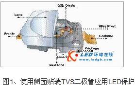
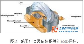
Figure 2 shows how the ESD protection can be more tightly integrated by applying a silicon secondary mount between the LED and the leadframe. This configuration makes the LED form factor more compact; the secondary substrate replaces the traditional substrate used in the side-mounted LED module, providing an ESD protection rating of over 15kVHBM. The good thermal conductivity of the silicon secondary placement also helps the LED to be relieved due to the LED The stress caused by the difference in thermal expansion coefficient from the lead frame.