Chip Design Process (1) - Prologue
Currently, foreign integrated circuit design is very mature, with the latest technology reaching 7nm. The country is still in the development phase. Regarding the development of integrated circuits, there's limited information available online. For IC designers, understanding the entire process of IC design is crucial. However, there seems to be no detailed explanation of the entire process on the internet. It's usually summarized into four main sections: design, manufacturing, testing, and packaging. Some data are scattered, with only a single detail mentioned, while some just talk about using a tool software without specifying which part of the process it's used in, making it unclear which tools each process might use (this view is based on personal experience and may not be entirely accurate). Therefore, I've made a personal summary of the issues related to the IC design process that I've encountered so far. This summary isn't very accurate due to personal experience, and many details in the chip design process remain unknown, especially regarding wafer fabrication and packaging. Nonetheless, this is at least a relatively complete summary of the IC design process.
Forward and Reverse Chip Design
Currently, major design companies worldwide mainly focus on forward design, while reverse design is primarily used to check if other companies have plagiarized. Although the original purpose of chip reverse engineering was to prevent chips from being copied, it later evolved into a solution adopted by small companies to design chips faster and more cost-effectively. In recent years, more and more companies in China have gradually shifted towards forward design, reducing their reliance on reverse design. However, many companies in the early stages of development still rely on reverse design. This article begins with a summary of chip reverse design.
Chip Design Process (2) - Tools
"If you want to do something good, you must first sharpen your tools." With the continuous development of integrated circuits, whether for forward or reverse design, they are increasingly dependent on tools. Therefore, before discussing the design process, let's take a look at the main tools and auxiliary software we will use.
First, the Main Tool Software
When it comes to design tools, one cannot help but mention the three major EDA vendors: Cadence, Synopsys, and Mentor. The software from these companies covers almost all the tools available for the chip design process. Cadence's most important IC design tools include the Cadence IC series, such as IC 5141 (the latest version is IC617), NC_VERILOG (Verilog simulation), SPECTRE (simulation), and ENCOUNTER (automatic layout). Synopsys' most famous tools include its comprehensive design compiler, timing analysis tool Prime Time, and simulation tool HSPICE. Mentor's most well-known tools are Calibre (layout DRC and LVS check) and ModelSim (Verilog simulation).
These are the most commonly used tools for IC design, whether for forward or reverse design. Of course, as software versions are updated and iterated, the names of the software may change. In addition, these tools are mainly concentrated on Linux-based operating systems, particularly Red Hat. Therefore, knowledge of Unix/Linux operating systems is still necessary. These systems are very different from Windows. To learn to use these software, one must first understand the relevant knowledge of these operating systems. Some tools have Windows versions, such as HSPICE and ModelSim.
Second, Auxiliary Tool Software
In addition to the IC design tools from the three major EDA vendors, the software development environments of companies like Altera (Intel), Xilinx, and Keil Software are also indispensable tools in the IC design process. They are used for FPGA, microcontroller, and ARM chip development. This type of software will be useful in the development of CP test and chip application solutions.
Layout extraction tools, such as NetEditorLite and ChipAnalyzer, are mainly used for chip reverse design.
Algorithm design tools, like MATLAB, have a wide range of applications, but for chip design, they are more suitable for algorithm prototyping, such as communication algorithms.
PCB layout tools, including Altium Designer, Orcad, and Allegro, are widely used. Among them, Orcad and Allegro are the main software in the Cadence circuit system design kit, while Altium Designer is the most commonly used software, with its predecessor being Protel.
LabVIEW and digital source meter are primarily used for semi-automated testing of chip electrical parameters, especially for analog chips. Their purpose is for chip design companies to analyze sample chip parameters.
How to use these tools will be explained in the following articles. Note: There is no specific description of the software usage environment; generally, it is used in the Windows environment.
Chip Design Flow (3) - Reverse Design
Since I am more familiar with the reverse design of the chip, let's start with that. Below is a flowchart of the chip reverse design I have organized. Most of these processes have been done, but some parts are unfamiliar, such as layout, chip manufacturing, and packaging, which will be explained in detail in the next chapter.
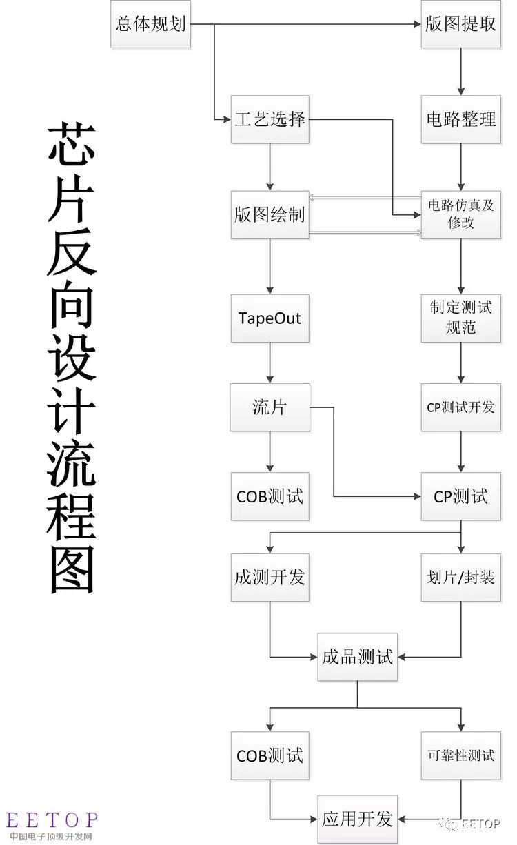
First, the Reverse Design Master Plan
At the early stage of developing a new chip, there must be a master plan for design. The most important question is whether the chip can bring benefits. After all, the company depends on products to survive. How to evaluate whether the chip can bring benefits? This requires years of experience to make an accurate assessment. Generally, it is to see which chips in the market are selling well, and sales in the next few years are bullish, and whether the company has the ability to design and sell channels. The chip costs I know to consider are as follows:
1. Chip filming costs;
2. The time cost of the chip from project to delivery, where the time process causes the chip to be designed, and the market is no longer needed;
3. The cost of filming;
4. The authorized use cost of the tool software;
5. Test costs, including CP test and finished product test and other costs required to build a test platform;
6. Packaging costs.
These considerations are not mature enough for me, but for me, it is enough for the time being. After making these costs an appropriate estimate, look at the benefits. For the income component, this is related to the market demand and sales trend. It needs to involve many other considerations. If the individual is not familiar with this piece, it will not comment. After the revenue problem is solved, it is clear that the project can be profitable, then it can be officially started. The pile of things mentioned above is actually part of the project feasibility analysis. However, in fact, some companies do not consider that much, because these feasibility analysis itself is very difficult. Which chip is reversed? Selecting a large company's chip for reverse will generally have a higher success rate. After the chip is selected, the film is taken. The chip is usually anatomically filmed between 1 week and 1 month, depending on the size of the chip.
Nickel Alkaline Battery,Solar Energy Battery,48V Nife Battery 200Ah ,Ni-Fe Battery 100~200Ah
Henan Xintaihang Power Source Co.,Ltd , https://www.taihangbattery.com