Programmable logic device PLD (Programmable Logic De-vice) is a digital circuit that can be programmed and configured by the user, using it to solve different logic design problems. The PLD consists of basic logic gates, flip-flops, and internal connection circuits that can be programmed using software and hardware (programmers) to implement specific logic functions. Programmable logic devices have undergone development from PROM, PLA, PAL, GAL to CPLDs and FPGAs since the early 1970s, with significant improvements in structure, process, integration, functionality, speed, and flexibility. And improve.
With the continuous update and replacement of digital integrated circuits, especially the emergence of programmable logic devices, the traditional digital system design methods have undergone fundamental changes. The flexibility of programmable logic devices allows hardware system designers to use a computer, a set of corresponding EDA software, and programmable logic chips in the lab to complete digital system design and production.
1 Introduction to Max+plusIIMax+plusII is a structure-independent, fully integrated design environment that allows designers to easily design input, fast processing, and device programming for Altera's various CPLD families. Max+plusII development system has a powerful processing capability and a high degree of flexibility, its main advantages: structure-independent, multi-platform, rich design library, open interface, fully integrated, support for multiple hardware description languages ​​(HDL), etc. .
The design of the digital system adopts a top-down, coarse-to-fine, step-by-step design method. The top-level circuit refers to the overall system requirements, and the bottom layer is the implementation of specific logic circuits. The top-down design method gradually decomposes a complex system into several functional modules to describe the design, and uses the EDA software platform to automatically complete the logic synthesis and optimization of each functional module, layout of the gate-level circuit, and then download to the hardware. In the design, the specific design process is as follows.
1.1 Design input
Max+plusII supports a variety of design input methods, such as schematic input, waveform input, text input, and their mixed inputs.
1.2 Design Process
After the design input is completed, the Max+plusII compiler is used to compile, check, and correct until the design input is correct. At the same time, the input file is logically simplified and optimized, and finally a programming file is generated. This is the core design aspect.
1.3 Design Check
Max+plusII provides designers with complete inspection method design simulation and timing analysis. Its purpose is to verify that the logic function of the circuit is correct, and at the same time to test the worst case delay of the target device. This error checking process is used to test combinational logic. The circuit's competitive risk and the timing, latency, etc. of the sequential logic circuits are critical.
1.4 Device Programming
After the circuit design and verification, Max+plusII's Program-mer downloads the compiled file generated by the compiler to a specific CPLD device, which is to achieve the physical programming of the target device.
2 Take the counter as an example to introduce a specific design methodCounters are very commonly used sequential logic circuits. There are many types of counters, and there are many ways to implement counters. You can buy most types of mid-scale integrated counters directly, and you can use triggers to set up counters that meet your needs. However, the counters implemented by the above methods are not flexible enough and cannot be modified at any time, and their versatility is poor. Here is how to implement a programmable logic device.
2.1 Design input
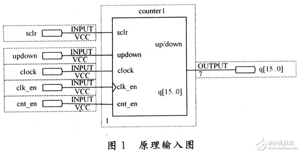
The idea of ​​using principle-graph input is more suitable for people who have been using traditional design methods. The schematic input is shown in Figure 1.
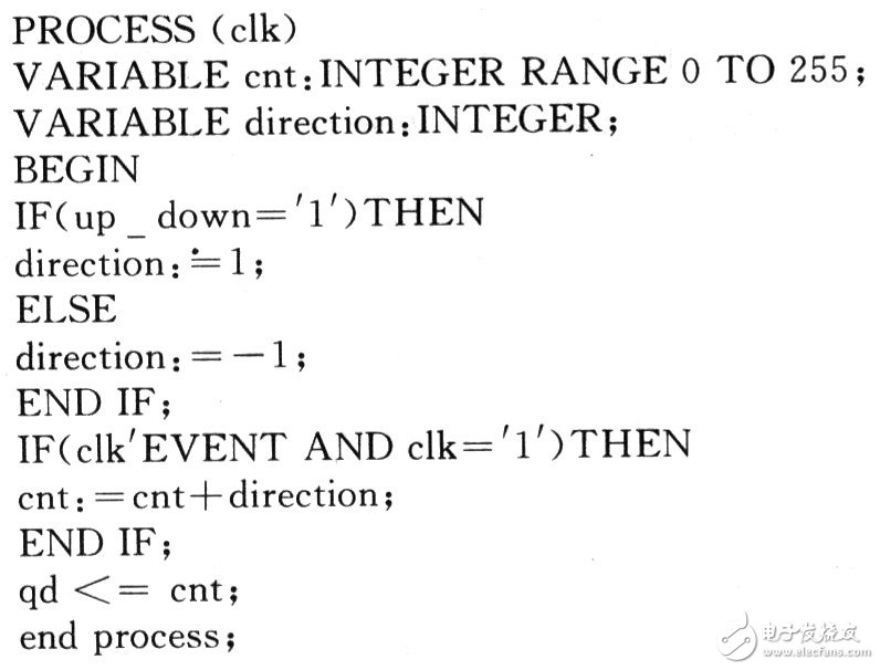
Methods using hardware description language input make it easier to get started and easier to modify for people without traditional design method experience. An implementation example of an up-down counter is given. The core parts of the program are as follows:
2.2 Design Process
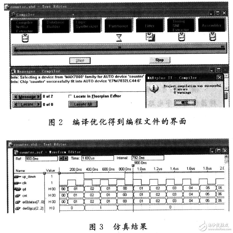
After the schematic or program is completed, select the device and pin definition, and then compile and optimize the interface of the programming file shown in Figure 2.
2.3 Design Check
After compiling, the waveform file is created for simulation. Note that the waveform file needs to be saved first. Saving the file name and the source file are the same for simulation. The result is shown in Figure 3.
The simulation results meet the design goals and meet the design requirements. At this time, you can compile the generated *. Download the pof file to the selected device. The device implemented by the above method is very convenient to modify, only need to modify the program to recompile and download, any type of counter can be implemented in the programmable logic device.
3 ConclusionWith the rapid development of electronic technology, CPLD and FPGA devices have been able to meet the requirements of most applications in terms of integration, functionality, and performance (speed and reliability). Using CPLD, FPGA and other large-scale programmable logic devices to replace the traditional standard integrated circuits, interface circuits and application-specific integrated circuits has become an inevitable trend of technological development. Programmable logic devices are the fastest growing class of devices in the logic device family. They appear to shorten the product development cycle, provide good on-site flexibility, and reduce development risk. With the continuous development of processes, technologies, and markets, the price of PLD products It will be more and more cheap, the integration is getting higher and higher, the speed is getting faster and faster, plus its design and development adopts powerful universal EDA tools that conform to international standards, and the application prospects of programmable logic devices will become more and more broad.
Wireless Bridge,Wifi Wireless Bridge,Gigabit Wifi Bridge,Long Range Wifi Bridge
Shenzhen MovingComm Technology Co., Ltd. , https://www.movingcommiot.com